Electronic Photosensitive Body and Manufacturing Method for Same, as well as Image Forming Apparatus
a manufacturing method and photosensitive technology, applied in the direction of electrographic process, photosensitive materials, instruments, etc., can solve the problems of rising manufacturing cost, achieve high film formation rate for the photosensitive layer, and reduce the amount of material gas used
- Summary
- Abstract
- Description
- Claims
- Application Information
AI Technical Summary
Benefits of technology
Problems solved by technology
Method used
Image
Examples
example 1
[0105]In the present example, the characteristic energy of the photoconductive layer in an electronic photosensitive body was evaluated.
[0106](Fabrication of Electronic Photosensitive Body)
[0107]An electronic photosensitive body was fabricated by forming only a photoconductive layer on a cylindrical base under the conditions shown in the following Table 1.
TABLE 1Photoconductive layerSampleSampleSampleSampleSample12345materialSiH4 (sccm)340340340340340gasesH2 (sccm)200200200200200B2 H6(sccm)0.30.30.30.30.3CH4 (sccm)00000pressure (Pa)8080808080base temperature (° C.)320320320260260direct current voltage−670−740−900——(V)RF power (W)———150300film thickness (μm)2020202020
[0108]A cylindrical base having an outer diameter of 84 mm and a length of 360 mm made substantially of aluminum was used.
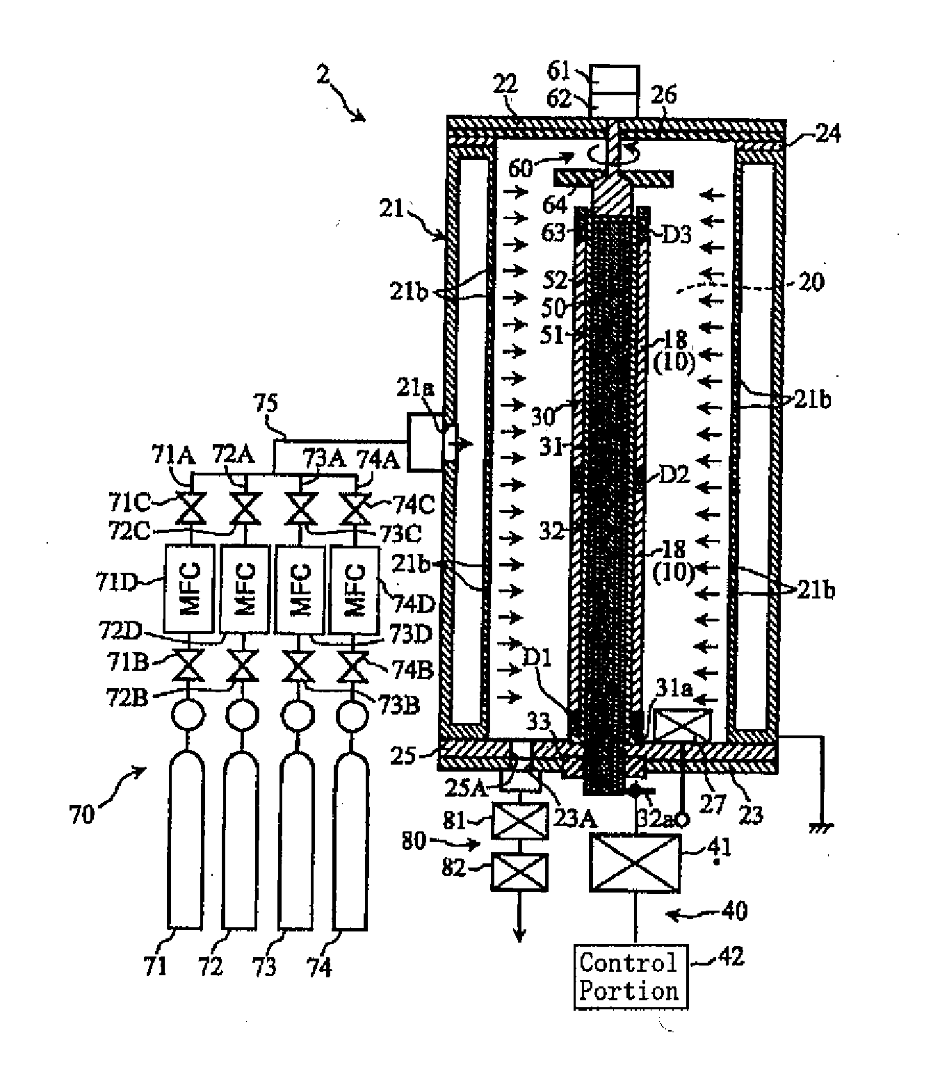
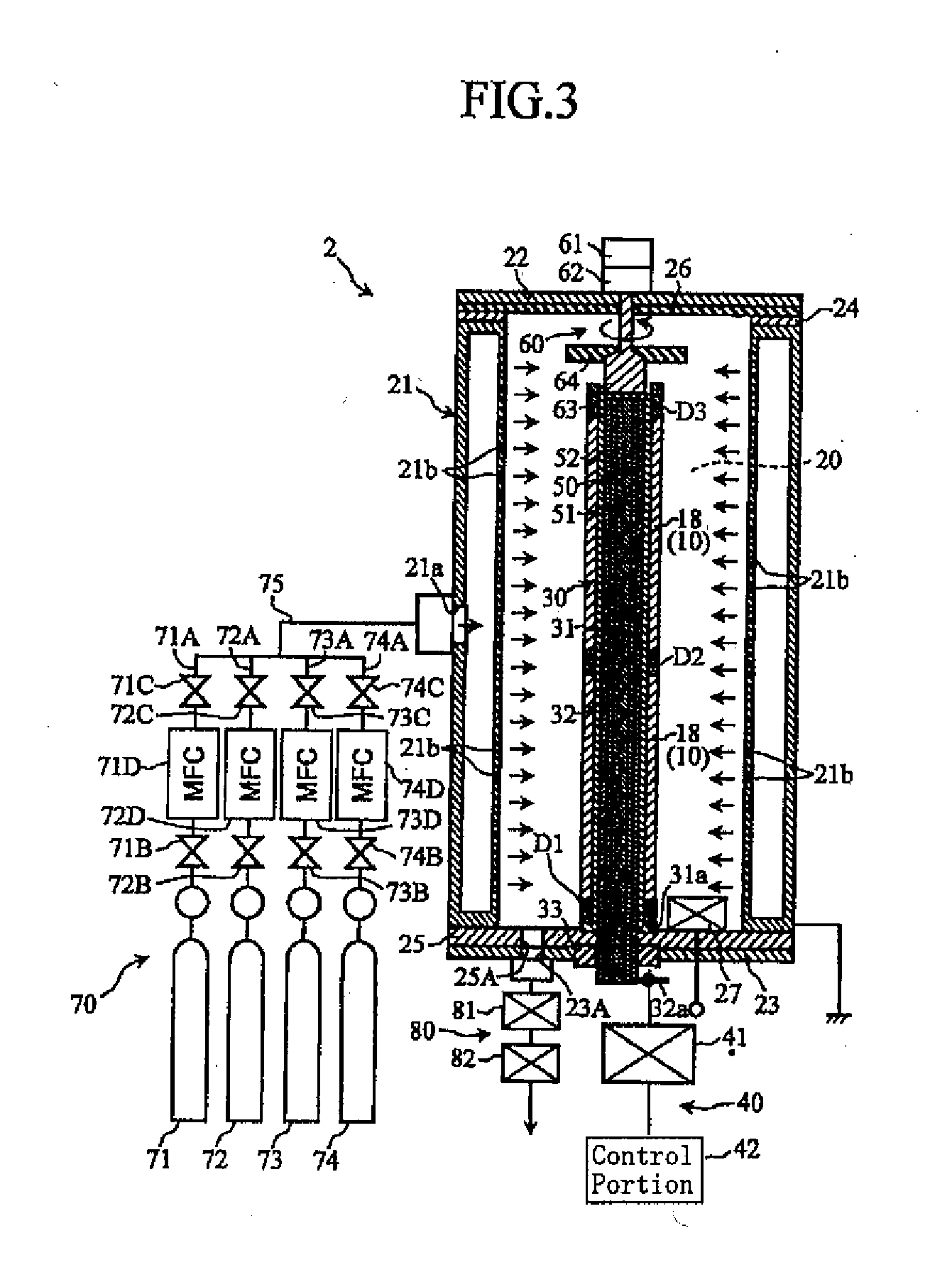
[0109]In Samples 1, 2 and 3, the photoconductive layers were formed using the plasma CVD unit 2 shown in FIG. 3. The direct current voltage was a direct current voltage in pulse form having a pulse fr...
example 2
[0119]In the present example, the effects of the characteristic energies E1 and E2 of the photoconductive layer for light for exposure and light for static elimination on the memory properties in electronic photosensitive bodies were examined. In addition, in the present example, the voltage for charging electronic photosensitive bodies and the speed of film formation for the photoconductive layer were also evaluated.
[0120](Fabrication of Electronic Photosensitive Bodies)
[0121]Electronic photosensitive bodies were formed by layering a charge injection blocking layer, a photoconductive layer and a surface layer in sequence on top of a cylindrical base. In Samples 1, 2, 3, 4 and 5, the charge injection blocking layer was formed under the conditions shown in the following Table 3, the photoconductive layer was formed under the conditions shown in the above Table 1, and the surface layer was formed under the conditions shown in the following Table 4. In Sample 6, the charge injection bl...
PUM
| Property | Measurement | Unit |
|---|---|---|
| Wavelength | aaaaa | aaaaa |
| Wavelength | aaaaa | aaaaa |
| Energy | aaaaa | aaaaa |
Abstract
Description
Claims
Application Information


