Integration substrate with a ultra-high-density capacitor and a through-substrate via

a technology of through-substrat via and integrated substrate, which is applied in the direction of solid-state devices, basic electric elements, electric devices, etc., can solve the problems of not cost-effective, large number of required passive components, and complicated processing, and achieves high capacitance density, simplifies the introduction of the integration device, and is easy to introduce into the existing production line

Active Publication Date: 2010-09-30
MURATA INTEGRATED PASSIVE SOLUTIONS
View PDF5 Cites 91 Cited by
  • Summary
  • Abstract
  • Description
  • Claims
  • Application Information

AI Technical Summary

Benefits of technology

[0026]In a further embodiment, the dielectric layers of the trench capacitor are made of for instance SiO2 or Si3N4 or silicon oxynitride. These materials are also used in other processes during the fabrication of integrated-circuit devices and are therefore compatible with well known and established processing technology. The integration-substrate of this embodiment is therefore particularly simple to introduce into an existing production line. Of course, other dielectrics, in particular higher-k dielectric layers such as PLZT and TaO2 can be used as alternatives or in combination with standard materials, in particular for open through-wafer trenches. They can be deposited by known techniques, for instance by atomic layer deposition (ALD). But such high-k materials are not required in the present trench capacitor for achieving a high capacitance density. This an advantage over existing technologies in the semiconductor industry for integrated capacitors with high-capacitance densities. High-k materials require extra processing for their integration in order to avoid, for instance, incorporation of material traces from these materials as undesired impurities into other functional device layers. Many metal elements contained in high-k dielectrics are known to form undesired so called deep-level impurities in semiconductor materials such as silicon.
[0027]Similarly, the capacitor-electrode layers are preferably made of polycrystalline silicon (polysilicon). Polysilicon is another IC-compatible material that further simplifies the introduction of the integration device into a production process.
[0028]The lateral extension of the respective openings for the trench capacitor and the through-substrate via are in one embodiment even larger than 15 micrometer. In a further embodiment, their lateral extension exceeds 20 micrometer. This way, capacitors with a particularly high capacitance density can be fabricated. For the larger lateral extension allows fabricating the trench filling with a larger number of layers in the alternating layer sequence of electrically conductive capacitor-electrode layers and dielectric layers. A suitable maximum lateral extension that may be used is, assuming a circular trench shape, a trench diameter of 80 to 100 micrometer. Calculations show that the achievable capacitance density of a multi-layer capacitor begins to saturate beyond this lateral extension.

Problems solved by technology

The large number of required passive components is a major factor in the assembly line production and yield.
However, the integration of such trench capacitors with high capacitance densities into a passive integration device for a system in package requires a rather complicated processing and is therefore not cost-effective.

Method used


Image

  • Integration substrate with a ultra-high-density capacitor and a through-substrate via
  • Integration substrate with a ultra-high-density capacitor and a through-substrate via
  • Integration substrate with a ultra-high-density capacitor and a through-substrate via

Examples


Embodiment Construction

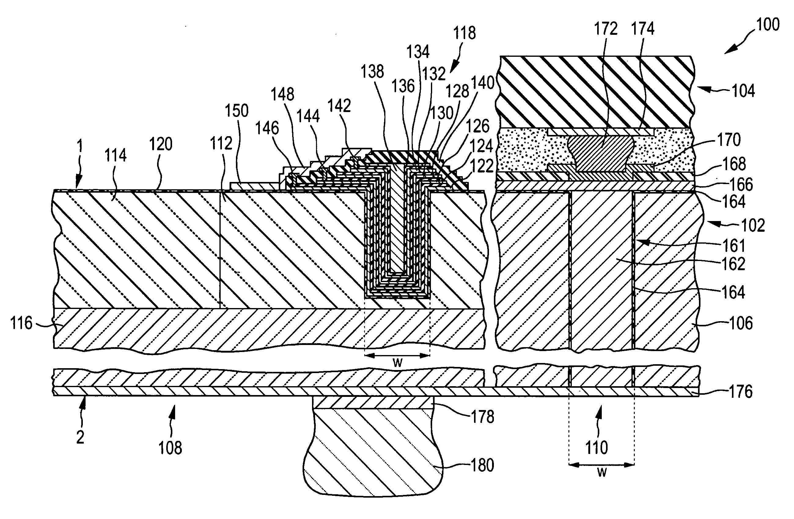
[0058]FIG. 1 shows a schematic cross sectional view of a stacked chip assembly 100 comprising an integration device in the form of an integration substrate 102 and an active die 104. The integration substrate 102 of this embodiment is based on a silicon substrate 106, and obtained from a high-ohmic silicon wafer. FIG. 1 shows two sections 108 and 110 of the integration substrate 102, which will also be referred to as the capacitor section 108 and the via section 110. Further details of the integration substrate are omitted, as are any details of the active die 104.

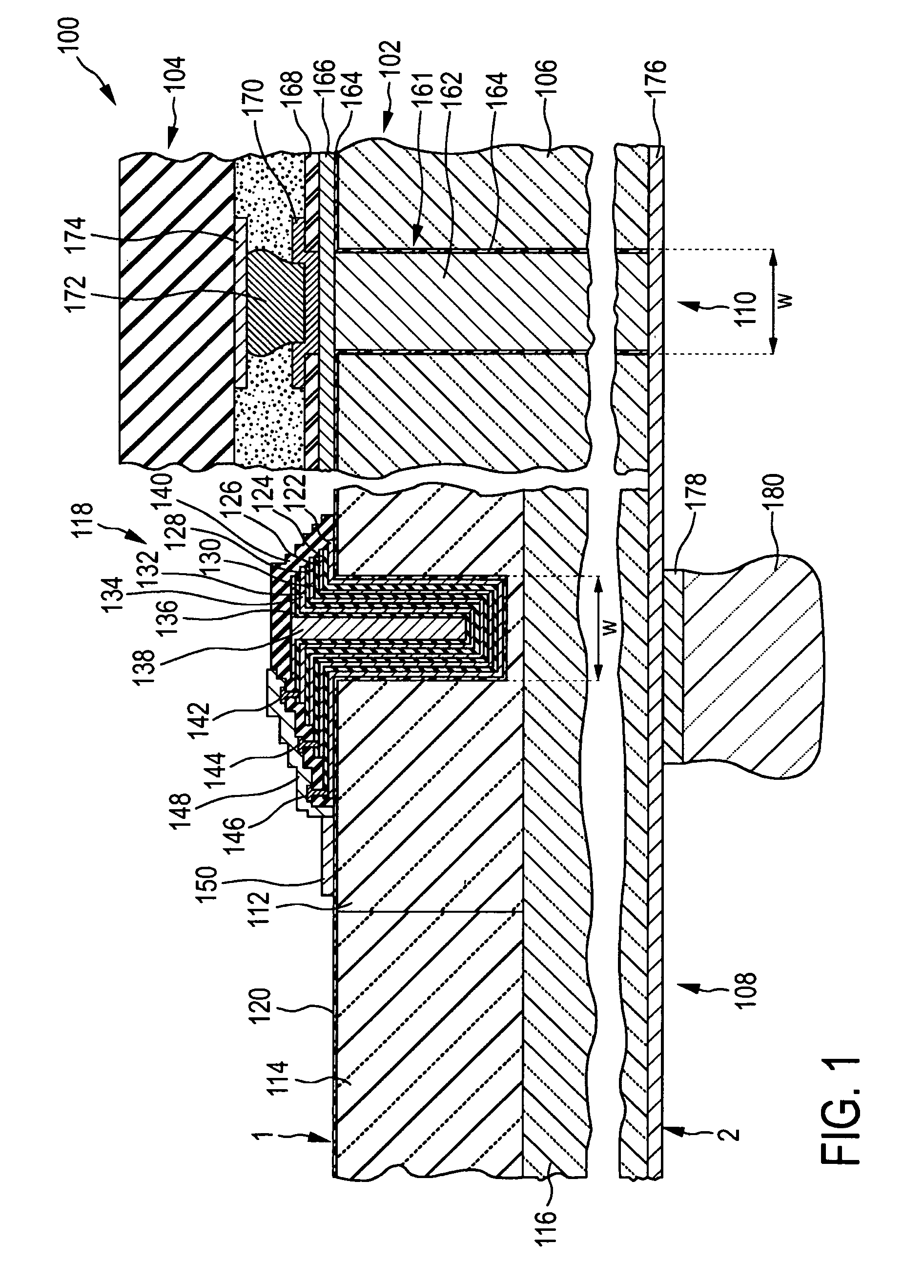
[0059]The following description will first turn to the capacitor section 108. In the capacitor section 108, doped wells 112 and 114 are provided on a first side 1 of the integration substrate. The depth of the doped wells 112 and 114 corresponds to that used in CMOS technology for providing regions of complementary conductivity. The well 112 serves for integration of a trench capacitor 118 into the integration substrate 10...


PUM


Abstract

An integration substrate for a system in package comprises a through-substrate via and a trench capacitor wherein with a trench filling that includes at least four electrically conductive capacitor-electrode layers in an alternating arrangement with dielectric layers. —The capacitor-electrode layers are alternatingly connected to a respective one of two capacitor terminals provided on the first or second substrate side. The trench capacitor and the through-substrate via are formed in respective trench openings and via openings in the semiconductor substrate, which have an equal lateral extension exceeding 10 micrometer. This structure allows, among other advantages, a particularly cost-effective fabrication of the integration substrate because the via openings and the trench openings in the substrate can be fabricated simultaneously.

Description

FIELD OF THE INVENTION[0001]The present invention relates to an integration device for a chip assembly such as a system-in-package. It further relates to a system-in-package containing an integration device, and to a method for fabricating an integration device.[0002]The disclosure of EP05110488.3, PCT / IB2006 / 054063 (PH001923EP1), and of EP06113955.6 (PH005924EP1) is enclosed by reference in its entirety in the present application.BACKGROUND OF THE INVENTION[0003]Electronic devices often consist of several individually packaged integrated circuits (IC) for different functions, e.g., logic circuits for information processing, memory for storing information, and I / O circuits for information exchange with the outside world. A System-in-Package or SIP is a device that incorporates multiple chips, which make up a complete electronic system, into a single package. In the stacked chip assembly of System-in-Package, all of the individual chips are assembled in a single package, which allows...

Claims


Application Information

Patent Timeline
Patent Type & Authority Applications(United States)
IPC IPC(8): H01L29/92H01L21/02
CPCH01L23/481H01L2224/73204H01L28/60H01L27/0805H01L28/90
Inventor KLOOTWIJK, JOHAN H.ROOZEBOOM, FREDDYRUIGROK, JAAPREEFMAN, DERK
Owner MURATA INTEGRATED PASSIVE SOLUTIONS
Why Eureka
Try Eureka