
Organic electroluminescent device and method for manufacturing the same

a technology of electroluminescent devices and organic materials, which is applied in the direction of layered products, printing, chemistry apparatuses and processes, etc., can solve the problems of insufficient full-scale study of practical implementation, difficult blue light emission, and inability to achieve full-scale study. , to achieve the effect of uniform light emission, increased covering effect relative to the organic layer, and high luminan

Inactive Publication Date: 2010-10-14
PANASONIC CORP
View PDF4 Cites 17 Cited by
  • Summary
  • Abstract
  • Description
  • Claims
  • Application Information

AI Technical Summary

Benefits of technology

[0017]In particular, in an organic electroluminescent device, a structure or a manufacturing step for realizing surface light emission is simple, and therefore, it is said that applications such as light emitting apparatus mounted with an organic electroluminescent device, backlight chiefly for spontaneous light emission type displays or liquid crystal displays, illumination of a surface light emission type or exposure apparatus applying an organic electroluminescent device as a light source are advantageous for realizing a low cost.
[0072]Also, a carrier balance can be adjusted, and for example, the light emission is realized on a center of the light emitting layer, whereby the breakage of the interface can be suppressed. Also, thermal deactivation of an exciton can be suppressed, and the organic electroluminescent device stably works and is excellent in a life characteristic.

Problems solved by technology

However, the inorganic electroluminescent devices involve a number of such problems that a voltage required for light emission is high as 100 V or more; that blue light emission is difficult; and that full-coloration by the three primary colors of RGB is difficult.
However, a full-scale study for practical implementation has not developed because the luminous efficiency is very poor.
However, in the manufacturing process, there is still no technique in the electrode formation as a substitute of the high-vacuum vapor deposition or sputtering method, and therefore, an enhancement of the productivity is hindered.
However, according to this method, it is necessary to achieve the deposition by previously bringing a cathode metal in a molten state into direct contact with an organic layer, and therefore, it was difficult to control the temperature of the electrode material or organic layer in itself for the purpose of keeping the molten state.
However, in view of the fact that it is necessary to inject a large charge for the purpose of obtaining a large quantity of light, there was also involved such a problem that the heat generation following the charge transfer accelerates the deterioration of an organic material and reduces the life.
For those reasons, though thickening of an electrode is an extremely useful measure, the conventional high vacuum thin film fabrication technology such as a vapor deposition method or a sputtering method involved such problems that the deposition rate is low and that the production cost is high.
Also, in order to obtain a large quantity of light, there was involved such a problem that the life is short because the luminous efficiency is low, and the driving voltage is high.
When the film thickness of the electron injection layer is less than 10 angstroms, the amount of the material having an electron injection function is so small that a sufficient electron injection characteristic cannot be imparted to the counter electrode.
On the other hand, when the film thickness of the electron injection layer exceeds 200 angstroms, the electron injection layer is so thick that bonding of the counter electrode in a solid plate form to the organic layer is disturbed.
Also, transparency of the electron injection layer is impaired.
On the other hand, when the work function of the electron injection layer exceeds 6.0 eV, a difference in the work function from the cathode which is the counter electrode becomes large, and therefore, favorable light emission is not obtainable.
On the other hand, when the average surface roughness Ra of the counter electrode exceeds 300 nm, there is a possibility that when the counter electrode is brought into contact with the organic layer, the counter electrode pierces through the organic layer, thereby generating a short circuit between the electrodes.
In the conductive polymer material, long molecular chains are complexly entangled with each other, and even when exposed to a high-temperature environment, the crystallization is not advanced as compared with low molecular weight materials which are used for general electroluminescent devices.

Method used


Image

  • Organic electroluminescent device and method for manufacturing the same
  • Organic electroluminescent device and method for manufacturing the same
  • Organic electroluminescent device and method for manufacturing the same

Examples


example 1

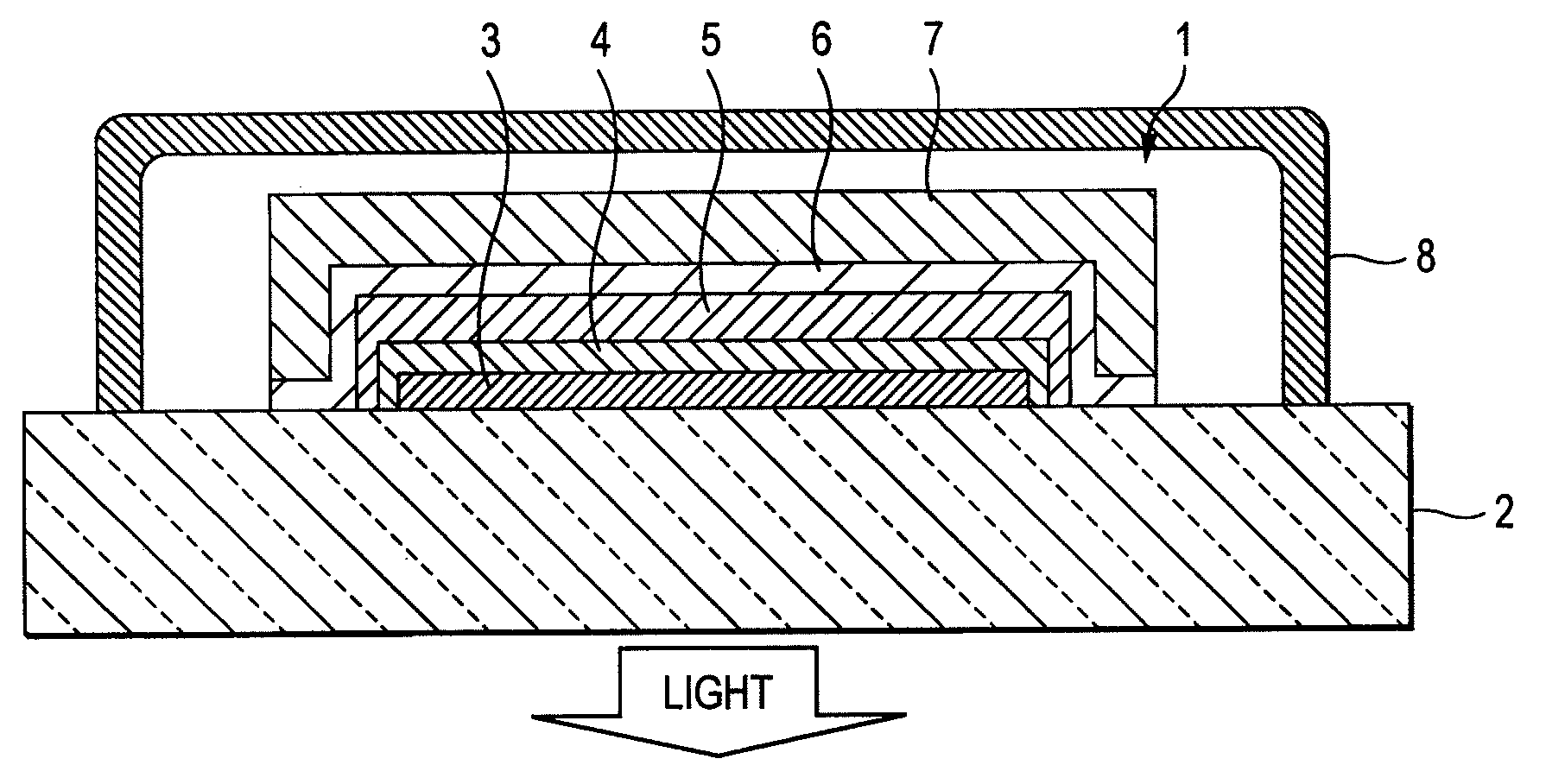
[0096]The structure of the organic electroluminescent device is hereunder described in detail with reference to FIG. 1.

(1) Substrate:

[0097]As the glass substrate 2 of FIG. 1, any material is useful so far as it has a mechanical or thermal strength and has a strength capable of holding an organic electroluminescent device. In the case where it is used as a surface from which light emission from the organic layer is extracted, any transparent or translucent material is useful so far as it has a function to effectively transmit light therethrough.

[0098]Also, though it is preferable that the glass substrate 2 is insulating, but there are no particular limitations. The glass substrate 2 may have conductivity within the range where the action of the organic electroluminescent device 1 is not hindered, or depending upon applications.

[0099]The glass substrate 2 is a colorless and transparent substrate as a first substrate. Examples of the glass substrate 2 which can be used include transpar...

example 2

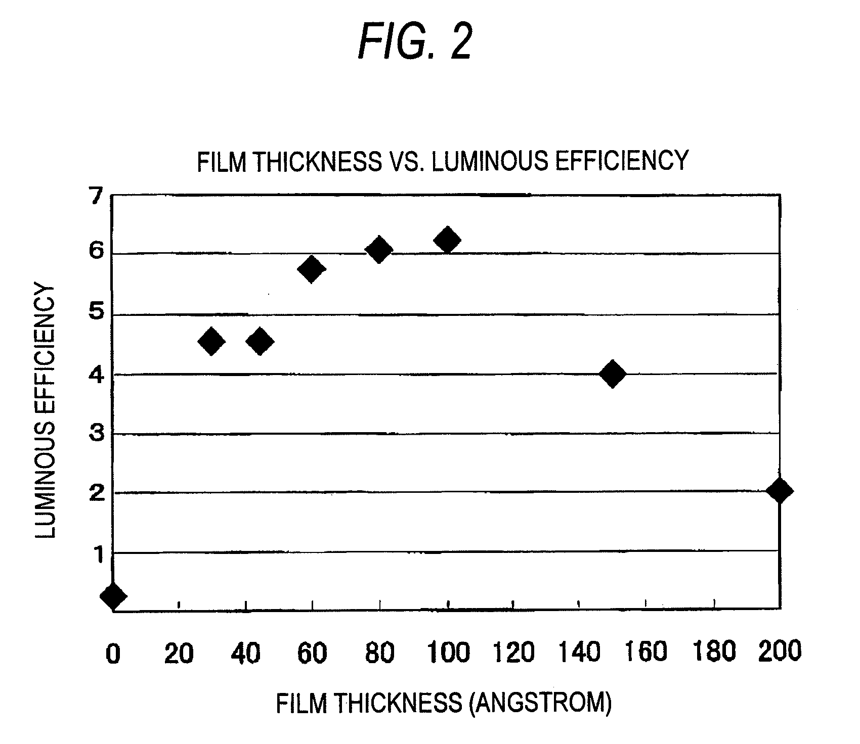
[0169]In the foregoing Example 1, zinc oxide as the metal oxide was deposited by adopting a sputtering method as the deposition method of the electron injection layer. However, in Example 2, for the purpose of realizing a preparation process of an organic electroluminescent device which does not require a high-vacuum process requiring a large amount of plant and equipment investment, such as a vapor deposition method or a sputtering method and which is able to significantly minimize the plant and equipment investment, the deposition of an electron injection layer made of a metal oxide was carried out by adopting a plating method which is a wet process for a method of depositing the electron injection layer.

[0170]According to Example 2, the electron injection layer deposited on the cathode 7 which is a counter electrode is an extremely thin film, and therefore, zinc deposited on the cathode 7 is oxidized in a bath or the atmosphere immediately after the plating treatment.

[0171]Accord...


PUM

PropertyMeasurementUnit
thicknessaaaaaaaaaa
thicknessaaaaaaaaaa
thicknessaaaaaaaaaa

Abstract

An organic electroluminescent device is provided, including at least one light emitting layer 5 composed of an organic material between a transparent electrode and a counter electrode, wherein the organic electroluminescent device includes an electron injection layer 6 previously provided on the organic layer side of the counter electrode which is contact disposed in a solid plate form on the organic layer and heat and pressure formed, and the electron injection layer 6 is constituted of a metal oxide. According to this configuration, it is possible to heat soften the counter electrode in a fixed plate form and join it, and it is possible to inexpensively manufacture the organic electroluminescent device 1 with ease.

Description

BACKGROUND[0001]1. Field of the Invention[0002]The present invention relates to an organic electroluminescent device and a method for manufacturing the organic device. In particular, the invention relates to an organic electroluminescent device which is an electroluminescent device to be driven over a wide luminance range of from a low luminance adopted for display devices and electronic appliances using an organic luminescent device as a light source to a high luminance for light source applications and the like and to a method for manufacturing the same.[0003]2. Description of the Related Art[0004]Electroluminescent devices are a light emitting device utilizing electroluminescence of a solid fluorescent substance, and inorganic electroluminescent devices using an inorganic material as a luminous body are put into practical use. At present, the electroluminescent devices are applied and spread to a backlight of a liquid crystal display, a flat panel display (FPD) and the like. Howe...

Claims


Application Information

Patent Timeline
Patent Type & Authority Applications(United States)
IPC IPC(8): H01L33/28H01L21/36B32B37/06B32B38/00
CPCH01L51/56H01L51/5092H10K50/171H10K71/40H10K71/12H10K71/00
Inventor YAMAMOTO, SHINYAMATSUO, NAOTO
Owner PANASONIC CORP
Features
  • Generate Ideas
  • Intellectual Property
  • Life Sciences
  • Materials
  • Tech Scout
  • Unparalleled Data Quality
  • Higher Quality Content
  • 60% Fewer Hallucinations
Learn More