Semiconductor device and method of manufacturing the same

a technology of semiconductor and tungsten, which is applied in the direction of semiconductor devices, transistors, electrical devices, etc., can solve the problems of high resistance of limited resistance reduction of the material used in the landing plug contact, and inability to commercialize the technology posterior to the gate and the bit line using tungsten (w)

Inactive Publication Date: 2010-10-28
SK HYNIX INC
View PDF34 Cites 1 Cited by
  • Summary
  • Abstract
  • Description
  • Claims
  • Application Information

AI Technical Summary

Benefits of technology

[0007]Various embodiments of the invention are directed to providing a semiconductor device and a method of manufacturing the same, which is capable of enhancing the processing speed of a semiconductor device, reducing the power consumption of a semiconductor device, and securing a sufficient process margin by reducing the resistance of gates, a bit line, and landing plug contacts.
[0008]According to an embodiment of the present invention, a semiconductor device comprises gates comprising a first conductive layer, landing plug contacts formed adjacent to the gate and formed of a second conductive layer, a bit line formed over the landing plug contacts and formed of a third conductive layer, and storage electrode contacts formed over the landing plug contacts and the bit line and formed of a fourth conductive layer. The first conductive layer, the second conductive layer, the third conductive layer, and the fourth conductive layer are made of the same material. Accordingly, since the resistance of the gates, the bit line, and the landing plug contacts is reduced, the processing speed of a semiconductor device can be increased and the power consumption of a semiconductor device can be reduced. Further, since a process of manufacturing a device is simplified, a process margin can be improved.
[0009]Further, the first conductive layer, the second conductive layer, the third conductive layer, and the fourth conductive layer are made of metal comprising copper (Cu). Accordingly, resistance can be minimized.

Problems solved by technology

However, technologies posterior to the gate and the bit line using tungsten (W) have not been commercialized, and there is a need for the development of a gate and a bit line using new materials.
Further, the material (i.e., polysilicon or tungsten) used in a landing plug contact has limitations in resistance reduction because it requires a high aspect ratio.
Consequently, there are problems in that the resistance of the landing plug contact is high and a gate Self-Aligned-Contact (SAC) fail frequently occurs with the smaller design rule of a semiconductor device.

Method used


Image

  • Semiconductor device and method of manufacturing the same
  • Semiconductor device and method of manufacturing the same
  • Semiconductor device and method of manufacturing the same

Examples


Embodiment Construction

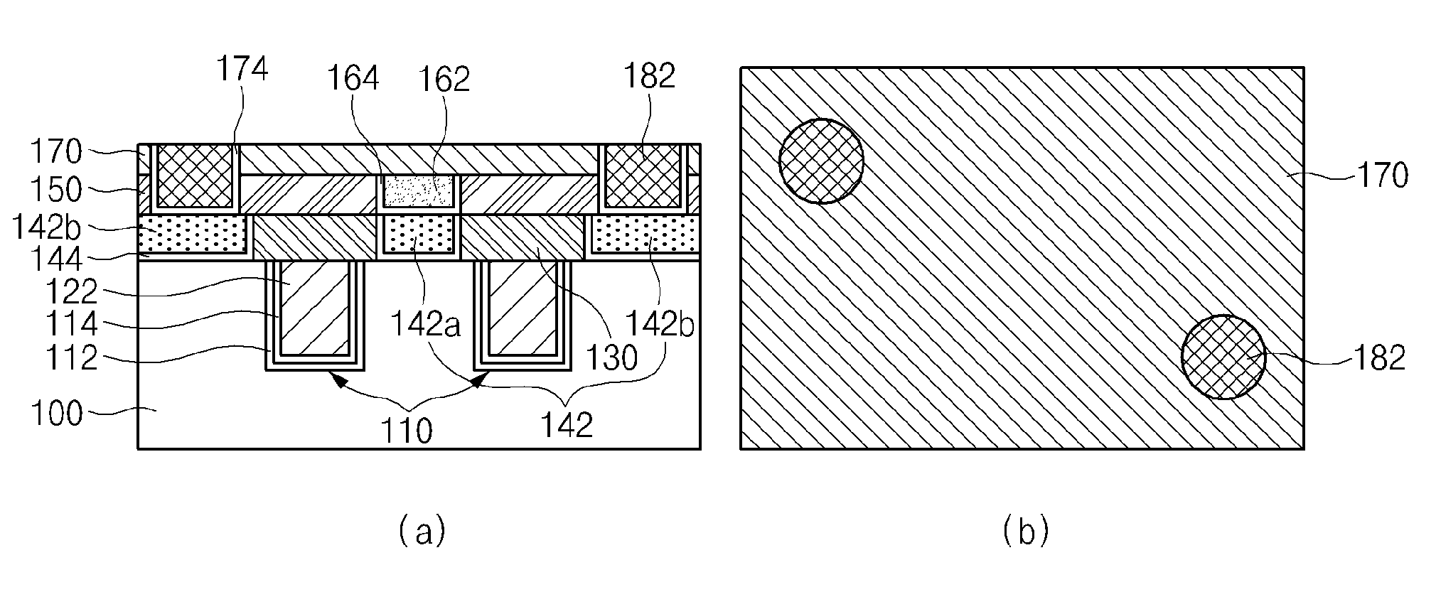
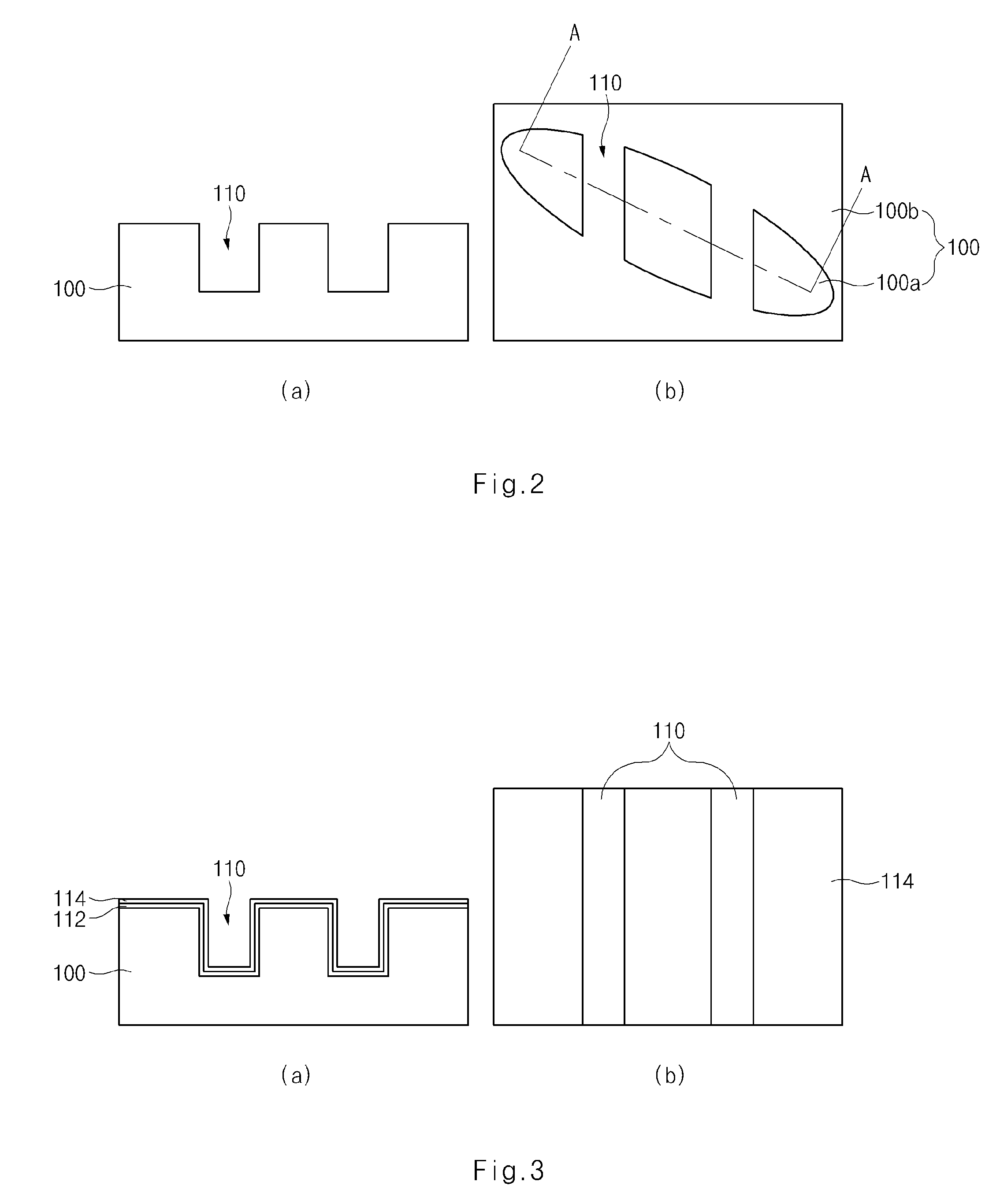
[0030]FIG. 1 is a cross-sectional view showing the structure of a semiconductor device according to an embodiment of the present invention. Referring to FIG. 1, recesses 110 are formed in a semiconductor substrate 100, and gate conductive layers 122 are buried in the respective recesses 110. A gate hard mask layer 130 is formed on the gate conductive layers 122. The gate conductive layer 122 and the gate hard mask layer 130 function as a gate electrode.

[0031]In the embodiment shown in FIG. 1, the gate is illustrated to be a recess gate formed by etching a surface of the semiconductor substrate 100 to a specific depth and then filling the etched portion with a gate material. Here, as shown in FIG. 1, the gate may be formed so that a top surface of the gate conductive layers 122 is identical to that of the semiconductor substrate 100 while the recess gate is formed.

[0032]This is because, in the embodiment shown in FIG. 1, the thickness of landing plug contacts 142a and 142b can be con...


PUM


Abstract

A semiconductor device comprises gates comprising a first conductive layer, landing plug contacts formed adjacent to the gate and formed of a second conductive layer, a bit line formed over the landing plug contacts and formed of a third conductive layer, and storage electrode contacts formed over the landing plug contacts and the bit line and formed of a fourth conductive layer. The first conductive layer, the second conductive layer, the third conductive layer, and the fourth conductive layer are made of the same material.

Description

CROSS-REFERENCE TO RELATED APPLICATION[0001]The present application claims priority to Korean patent application number 10-2009-0035174, filed on Apr. 22, 2009, which is incorporated by reference in its entirety.BACKGROUND OF THE INVENTION[0002]The present invention relates to a semiconductor device and a method of manufacturing the same.[0003]A semiconductor device is manufactured through a process of implanting an impurity into a specific region within a silicon wafer or depositing / etching a new material on the specific region within the silicon wafer. A representative example of the semiconductor device may include a semiconductor memory device. The semiconductor memory device includes a number of unit cells each including capacitors and transistors. The capacitor (in the case of DRAM) is used to temporarily store data. The transistor is used to transfer data between a bit line and a capacitor in response to a control signal (a word line). The transistor includes three regions; a...

Claims


Application Information

Patent Timeline
Patent Type & Authority Applications(United States)
IPC IPC(8): H01L27/10H01L21/336H01L21/3205
CPCH01L21/76843H01L27/10888H01L27/10876H01L27/10855H10B12/0335H10B12/053H10B12/485H01L21/28H10B99/00
Inventor JANG, CHI HWAN
Owner SK HYNIX INC
Why Eureka
Try Eureka