Methods of embedding thin-film capacitors into semiconductor packages using temporary carrier layers

a thin-film capacitor and semiconductor technology, applied in the field of semiconductor packages, can solve the problems of not revealing methods or specific materials that may be used, and limit the number of smt chip capacitors that can be mounted in parallel on a semiconductor package, and achieve the effect of improving structural support and minimal distortion

Active Publication Date: 2010-10-28
CHEMTRON RES
View PDF27 Cites 5 Cited by
  • Summary
  • Abstract
  • Description
  • Claims
  • Application Information

AI Technical Summary

Benefits of technology

[0011]Semiconductor packages constructed according to the above methods allow for improved structural support during printed wiring board processing which provides for minimal distortion or buckling of the thin-film capacitor.

Problems solved by technology

As semiconductor devices including integrated circuits (IC) operate at higher frequencies, higher data rates and lower voltages, noise in the power and ground (return) lines and supplying sufficient current to accommodate faster circuit switching become increasingly important problems requiring low impedance in the power distribution system.
There is, however, a limitation to the number of SMT chip capacitors that can be mounted in parallel on a semiconductor package because the package is not much larger than the IC itself.
However, Borland et al. does not disclose methods or specific materials that may be utilized.

Method used


Image

  • Methods of embedding thin-film capacitors into semiconductor packages using temporary carrier layers
  • Methods of embedding thin-film capacitors into semiconductor packages using temporary carrier layers
  • Methods of embedding thin-film capacitors into semiconductor packages using temporary carrier layers

Examples


example 1

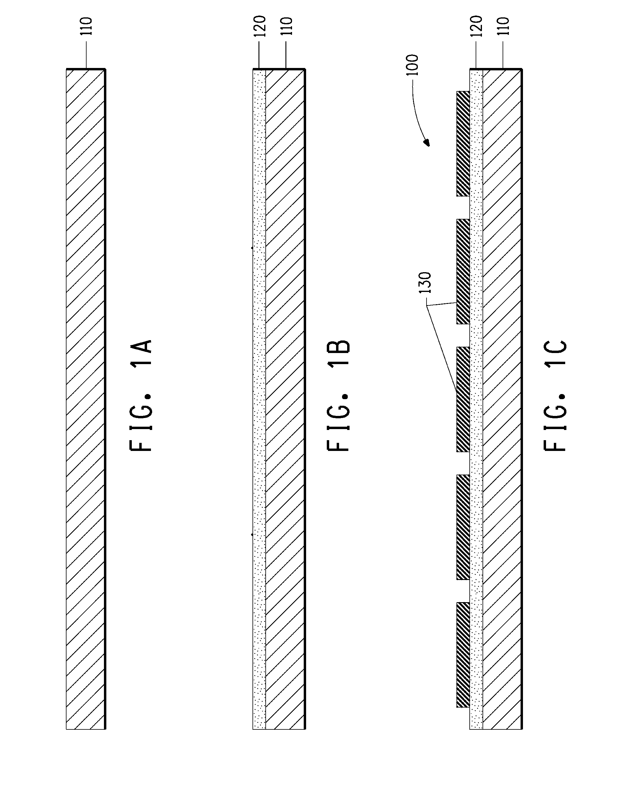
[0070]Three different types of magnetic sheet material were obtained from Magnum Magnetics, of Marietta, Ohio. One was 0.3 mm thick with a biaxially oriented polypropylene material on one of its sides. Another was 0.76 mm thick with a matte white material on one of its sides. A third was a higher magnetic strength material that was 0.76 mm thick with no other material on either side. A piece of each of these 3 types of magnetic sheet was placed in an oven set to a temperature of 190° C. for 30 minutes. Upon removal from the oven, all three magnetic material sheet types were warped and had blisters. A piece of each of the 3 types of magnetic sheet material was placed in an oven set to a temperature of 120° C. for 10 minutes. The 0.3 mm thick magnetic sheet and the 0.76 thick magnetic sheet with the matte white material on one of its sides were unaffected. The higher magnetic strength magnetic sheet sample with no additional material on either side exhibited some minor blisters.

example 2

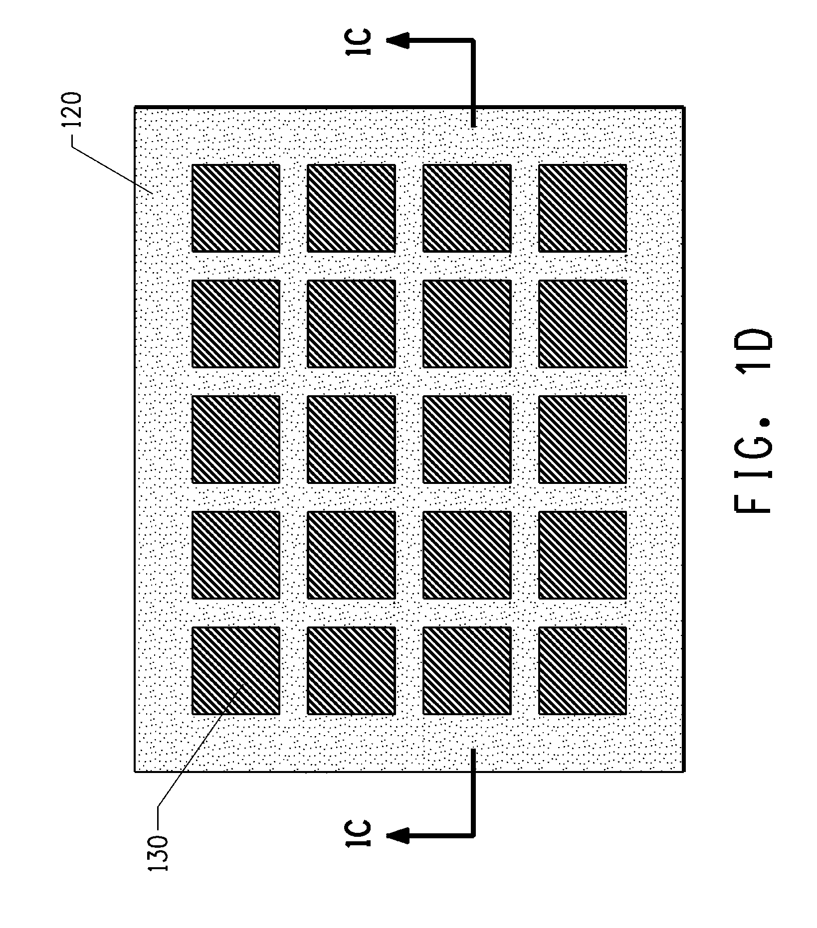
[0071]Pieces of the three types of magnetic sheets of Example 1 were sequentially exposed to potassium carbonate developer chemistry, cupric chloride etching chemistry and an alkaline, aqueous photoresist stripper chemistry at process temperatures typical in the printed wiring board industry. All of the samples were unaffected.

example 3

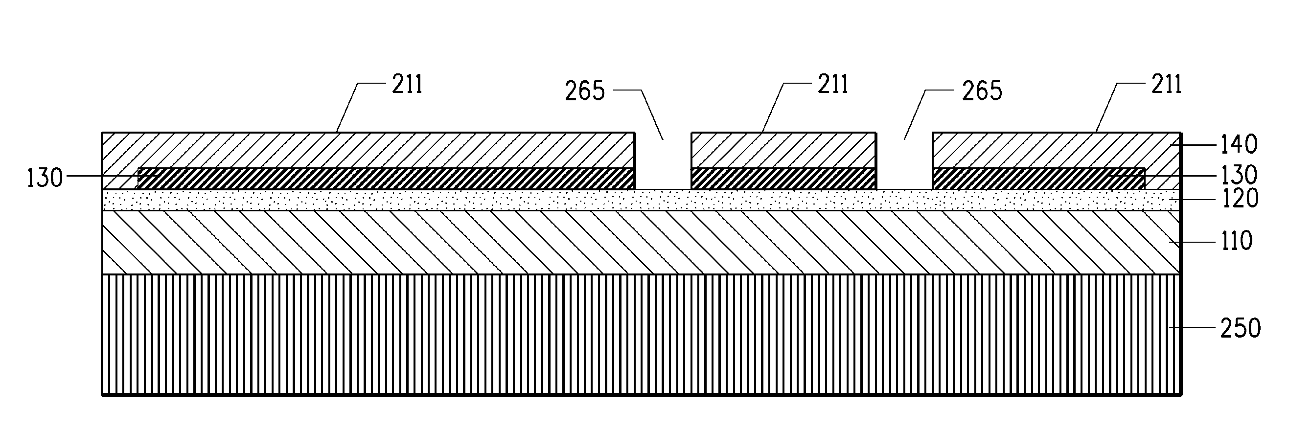
[0072]A 25 micrometer thick piece of nickel foil 270, obtained from Hamilton Precision Metals, of Lancaster, Pa., that had been processed through a fired-on-foil thin-film capacitor process without depositing the thin-film dielectric, was placed by hand on a piece of the 0.76 thick magnetic sheet material of Example 1 on the side opposite the white material. DuPont™ Riston® MX-5020 photoresist was laminated to the side of the nickel foil opposite to the magnetic sheet. The photoresist was exposed in an exposure unit typical in the printed wiring board industry to a Stouffer Step 9 exposure level and the coversheet was removed from the exposed photoresist. The sample was laser drilled using a UV laser. The sample was laser drilled with the laser initially impacting the photoresist side of the sample. The photoresist was applied to serve as a temporary means to protect the nickel surface from having any laser drilling residue deposited on the nickel surface. After laser drilling, the ...


PUM


Abstract

Disclosed are methods of making a semiconductor package comprising at least one thin-film capacitor embedded into at least one build-up layer of said semiconductor package. A thin-film capacitor is provided wherein the thin-film capacitor has a first electrode and a second electrode separated by a dielectric. A temporary carrier layer is applied to the first electrode and the second electrode is patterned. A PWB core and a build-up material are provided, and the build-up material is placed between the PWB core and the patterned second electrode of said thin-film capacitor. The patterned electrode side of the thin-film capacitor is laminated to the PWB core by way of the build-up material, the temporary carrier layer is removed, and the first electrode is patterned.

Description

[0001]Priority is claimed to U.S. Provisional Application No. 61 / 173,348 filed on Apr. 28, 2009, which is herein incorporated by reference.TECHNICAL FIELD[0002]The technical field relates to semiconductor packages and methods of incorporating thin-film capacitors into the build-up layers of a semiconductor package to provide low inductance power to the semiconductor device.BACKGROUND ART[0003]As semiconductor devices including integrated circuits (IC) operate at higher frequencies, higher data rates and lower voltages, noise in the power and ground (return) lines and supplying sufficient current to accommodate faster circuit switching become increasingly important problems requiring low impedance in the power distribution system. In order to provide low noise, stable power to the IC, impedance in conventional circuits is reduced by use of large numbers of surface mount technology (SMT) capacitors interconnected in parallel placed and as close to the IC as possible.[0004]High power a...

Claims


Application Information

Patent Timeline
Patent Type & Authority Applications(United States)
IPC IPC(8): H01L27/08H01L21/50
CPCH05K1/162H05K3/025H05K2201/0175H05K2201/0355H05K2203/104H05K2201/09309H05K2201/09536H05K2201/09718H05K2201/10674H05K2201/083H01L2224/16225
Inventor DELLIS, LYNNE E.DIETZ, KARL HARTMANNMCGREGOR, DAVID ROSS
Owner CHEMTRON RES
Why Eureka
Try Eureka