Method of forming highly conformal amorphous carbon layer

Active Publication Date: 2010-11-18
ASM JAPAN
View PDF28 Cites 26 Cited by
  • Summary
  • Abstract
  • Description
  • Claims
  • Application Information

AI Technical Summary

Benefits of technology

[0018]In an embodiment, in order to form an amorphous hydrogenated carbon layer, as the hydrocarbon-containing precursor, a hydrocarbon-containing precursor (CαHβXγ, where α and β are natural numbers, γ is an integer including zero; X is O, N or F) may be used. In an embodiment, γ is zero. Helium may be used as the carrier gas since it is easily ionized and is advantageous for initiating a plasma in a chamber with a low risk of arcing. The additional gas may be selected from the group consisting of He, Ar, Kr, Xe, and the molar

Problems solved by technology

Such thin resist layers can be insufficient to mask underlying material layers during the pattern transfer step due to attack by the chemical etchant.
However, current deposition processes for amorphous carbon hardmask result in poor step coverage and/or non-conformal sidewall protection of the hardmask on the uneven surface of the substrate making successful pattern transfer increasingly difficult as pattern densities continue to shrink.
During rework process, the surface of the underlying layer, amorphous carbon hardmask layer, may be attacked by the etchant used to remove the resist mask, thereby causing thickness of the hardmask to be reduced or the profile of the har

Method used


Image

  • Method of forming highly conformal amorphous carbon layer
  • Method of forming highly conformal amorphous carbon layer
  • Method of forming highly conformal amorphous carbon layer

Examples


example

Resist Pattern for Double Patterning

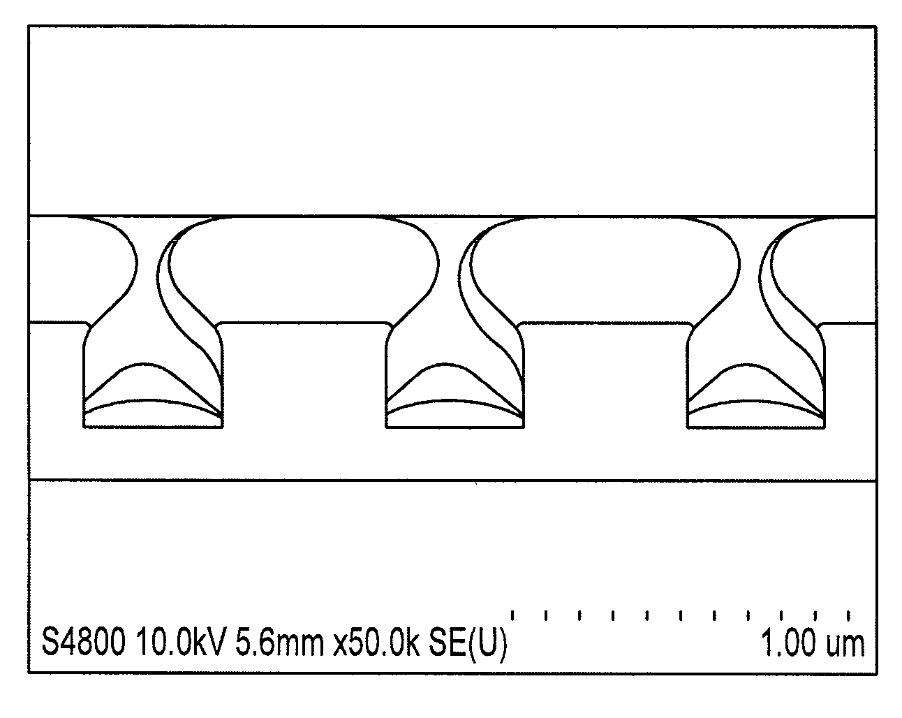
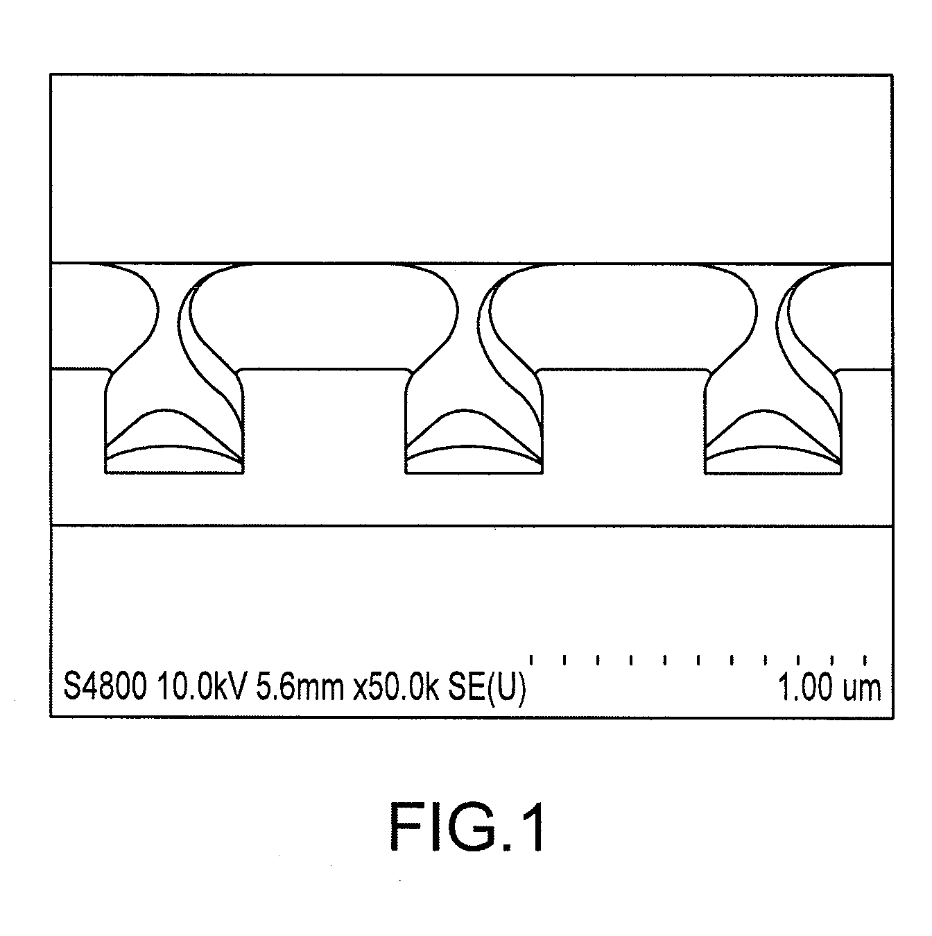
[0118]Another advantage of an conformal amorphous carbon deposition process is that a lower temperature process may be used as sacrificial layer on a resist pattern for double patterning technology.

[0119]For forming conformal amorphous carbon layer on a resist pattern, deposition conditions in embodiments may be as follows:

[0120]Isoprene: 10˜300 sccm (preferably 100˜120 sccm)

[0121]Argon: 0˜3000 sccm (preferably 400˜600 sccm)

[0122]Nitrogen: 0˜1000 sccm (preferably 400˜600 sccm)

[0123]Process helium: 3000 sccm

[0124]Sealed helium: 50 sccm

[0125]Carrier helium: 300 sccm

[0126]Substrate temperature: 0˜150° C. (preferably 0˜50° C.)

[0127]RF power: 0.02 W / cm2˜7 W / cm2 (including a range of 0.05˜5 W / cm2, and a range of 0.5˜3 W / cm2 in embodiments).

[0128]Pressure: 0.1˜10 Torr (preferably 5˜6 Torr)

[0129]Deposition time: 30 sec.

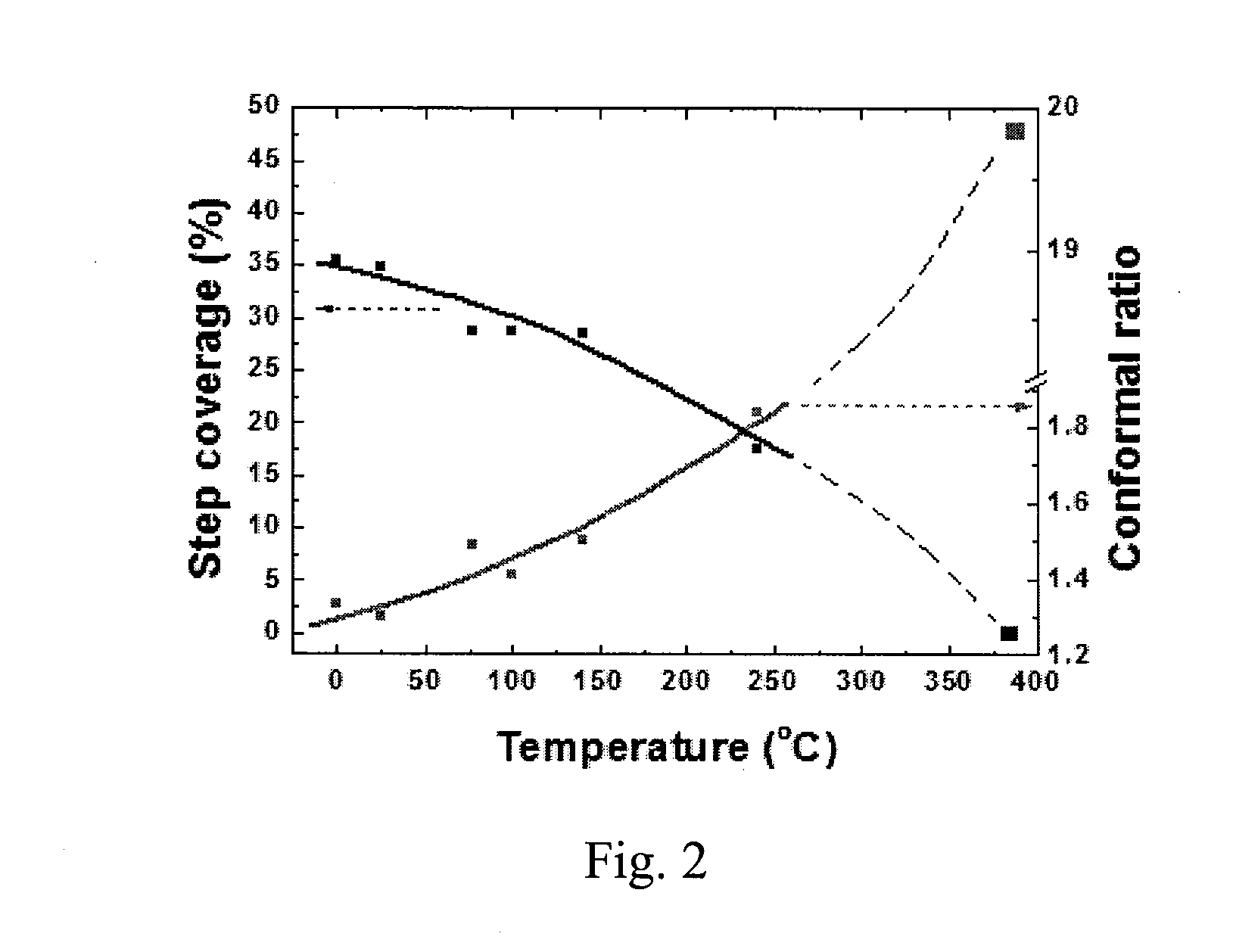
[0130]The obtained amorphous carbon film differ, depending on the process conditions, in an embodiments, shows a step coverage of more tha...


PUM

PropertyMeasurementUnit
Temperatureaaaaaaaaaa
Fractionaaaaaaaaaa
Pressureaaaaaaaaaa

Abstract

A method of forming a conformal amorphous hydrogenated carbon layer on an irregular surface of a semiconductor substrate includes: vaporizing a hydrocarbon-containing precursor; introducing the vaporized precursor and an argon gas into a CVD reaction chamber inside which the semiconductor substrate is placed; depositing a conformal amorphous hydrogenated carbon layer on the irregular surface of the semiconductor substrate by plasma CVD; and controlling the deposition of the conformal ratio of the depositing conformal amorphous hydrogenated carbon layer. The controlling includes (a) adjusting a step coverage of the conformal amorphous hydrogenated carbon layer to about 30% or higher as a function of substrate temperature, and (b) adjusting a conformal ratio of the conformal amorphous hydrogenated carbon layer to about 0.9 to about 1.1 as a function of RF power and/or argon gas flow rate,

Description

BACKGROUND[0001]1. Field of the Invention[0002]The present invention relates to semiconductor integrated circuit manufacturing and, more particularly to a method of forming a conformal amorphous carbon layer suitable for etching processes and double patterning processes.[0003]2. Description of the Related Art[0004]Integrated circuits fabricated on semiconductor substrates for large scale integration require multiple levels of metal interconnections to electrically interconnect the discrete layers of semiconductor devices on the semiconductor chips. The different levels of interconnections are separated by various insulating or dielectric layers, which have been etched via holes to connect one level of metal to the next.[0005]The evolution of chip design continually requires faster circuitry and greater circuit density. The demands for faster circuits with greater circuit densities impose corresponding demands on the materials used to fabricate such integrated circuits. In particular...

Claims


Application Information

Patent Timeline
IPC IPC(8): H01L21/66
CPCH01L21/02115H01L21/3146H01L21/0337H01L21/02274
Inventor LEE, WOO-JINFUKAZAWA, ATSUKI
Owner ASM JAPAN
Why Eureka
Try Eureka