Lateral collection architecture for sls detectors

a detector and lateral collection technology, applied in semiconductor devices, solid-state devices, nanotechnology, etc., can solve the problems of inherently difficult passivation process of sls detectors, degrade the performance of the photodiode, and the foregoing photodiode architecture suffers from a number of problems, so as to promote the lateral collection of photogenerated charge carriers, enhance the lateral mobility of carriers, and improve the effect of fill factor

Active Publication Date: 2010-12-02
TELEDYNE SCI & IMAGING
View PDF3 Cites 16 Cited by
  • Summary
  • Abstract
  • Description
  • Claims
  • Application Information

AI Technical Summary

Benefits of technology

[0009]The present invention provides a planar architecture for a photodetector having one or more photodiode junctions oriented transversely within an SLS structure to promote lateral collection of photogenerated charge carriers. The photodiode junctions are formed in selected regions by diffusing a dopant that changes the carrier type of the superlattice in the selected regions. The transverse orientation of the photodiode junctions exploits the naturally enhanced lateral mobility of carriers in an SLS to achieve higher fill factor. Passivation requirements are eliminated by eliminating the sidewall and by terminating the metallurgical diode junctions at the top surface of the photodetector within wide bandgap material which is relatively resistant to dark current generation. As a result, the invention achieves an increase in the ratio of photocurrent to dark current, and higher quantum efficiencies. The diffusion process may also homogenize the superlattice in the region of the diffusion widening the band gap and further reducing dark currents from that region. For appropriate shallow-depth structures, where the needed junction depth is on the order of 1.5 microns or less, implantation may substitute for diffusion. In this situation, the heavy doping of the implanted region would reduce minority carrier concentration to offset the effects of implant-induced damage to avoid increasing dark current.

Problems solved by technology

The foregoing photodiode architecture suffers from a number of problems.
Notably, the exposed sidewalls of the mesa (29) can be a source of undesirable excess currents that degrade the performance of the photodiode 11.
In addition, the passivation process itself can be inherently difficult for an SLS detector, especially for detectors that have bare surface mesa geometries.
To date, sidewall passivation techniques have not been completely effective.
Aside from the passivation layer, SLS detectors have other characteristics that inhibit the design of practical detector architecture.
One problem is that SLS detectors can exhibit poor quantum efficiency (QE), i.e. the fraction of incident photons registered by the detector.
This is mainly the result of poor minority carrier mobility perpendicular to the plane of the superlattice and short minority carrier lifetime.
Another problem is that SLS detectors can exhibit undesirable variations in dark current and shunting effects.

Method used


Image

  • Lateral collection architecture for sls detectors
  • Lateral collection architecture for sls detectors
  • Lateral collection architecture for sls detectors

Examples


Embodiment Construction

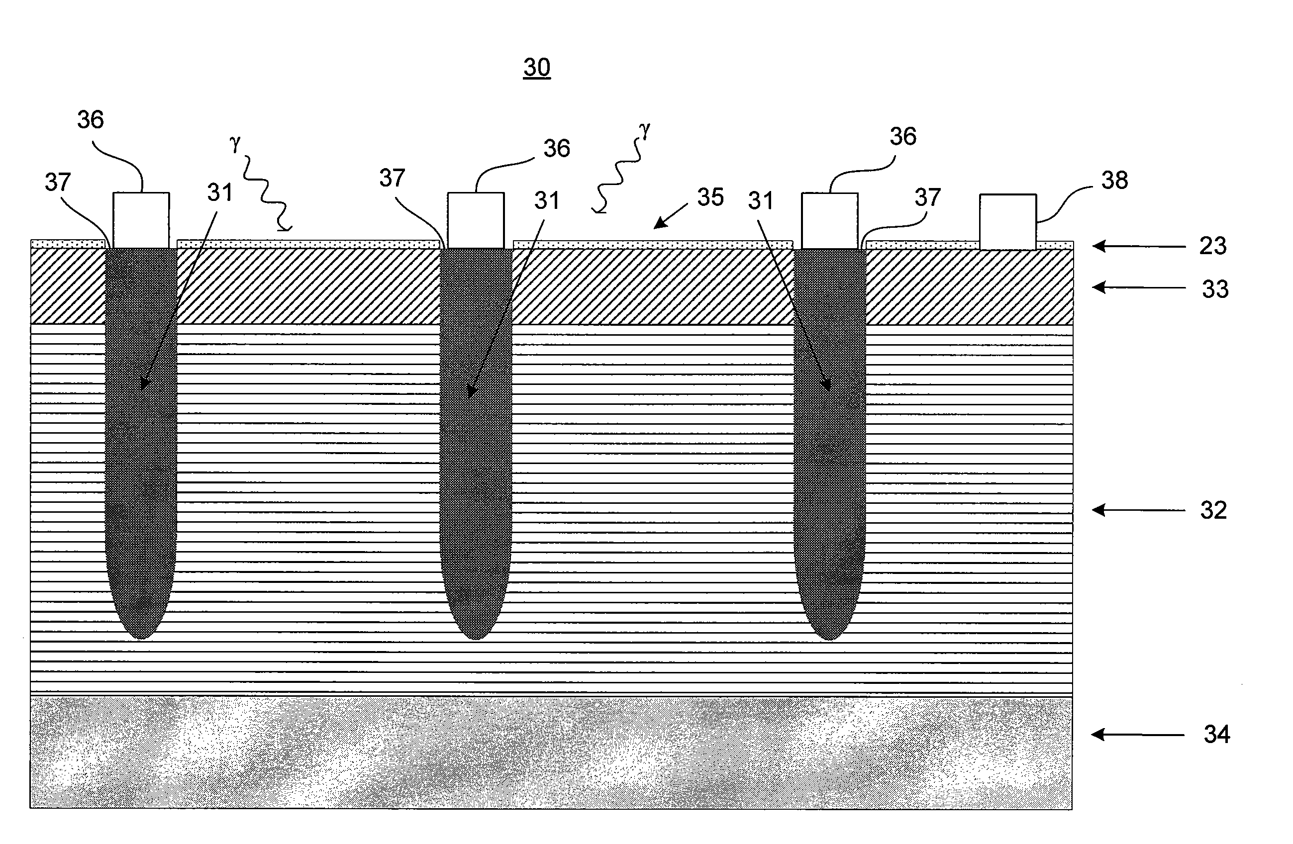
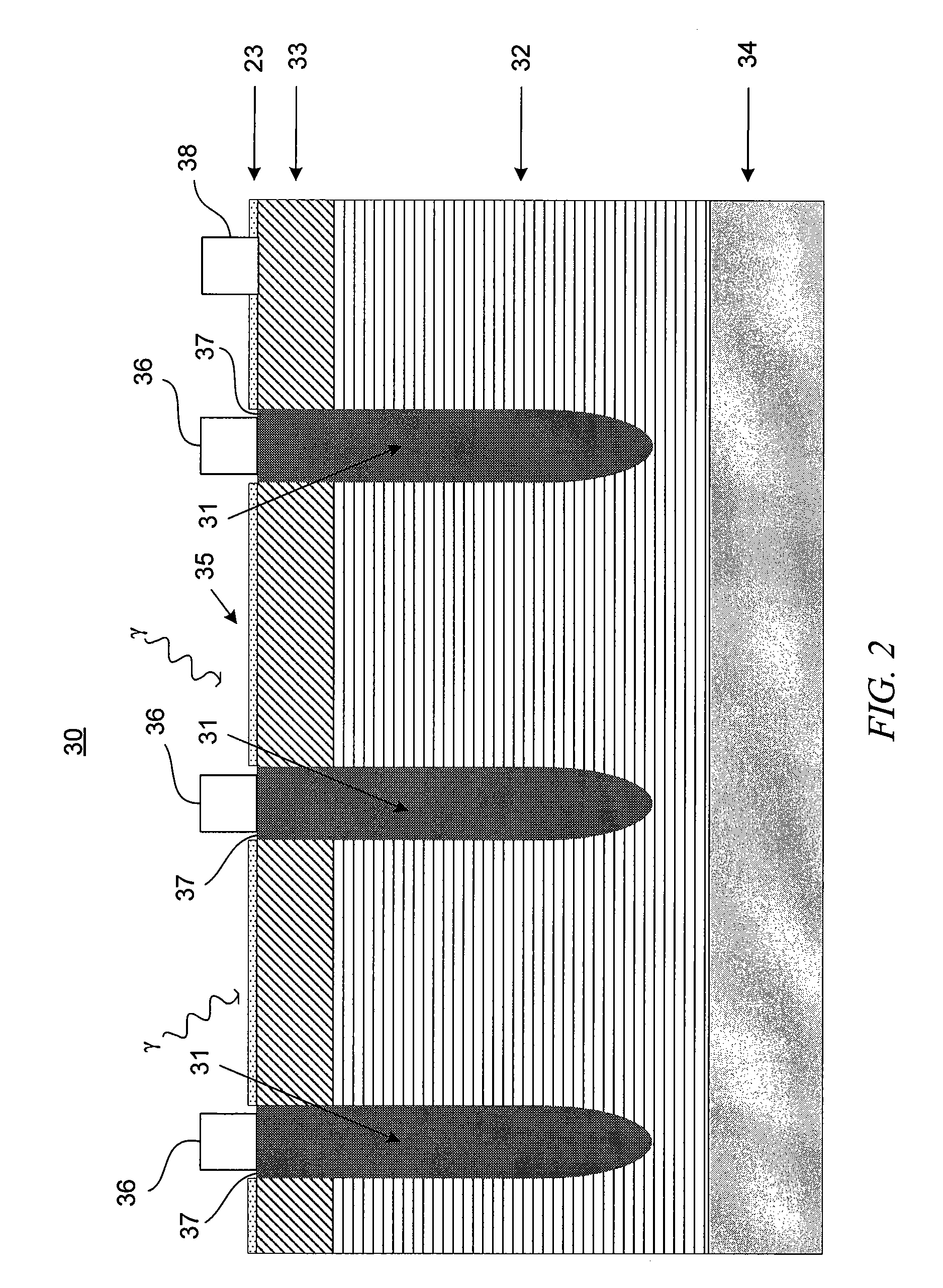
[0050]This disclosure presents exemplary embodiments of the invention of lateral collection architecture for quantum confined diode structures (e.g., SLS photodetectors, layers or structures, quantum dots, etc.). This architecture has particular application for fabricating photodiode arrays and provides a superior alternative to conventional mesa-etched designs. The invention introduces the concept of forming planar photodiodes from SLS structures of a single carrier type (n or p) by diffusing or implanting dopants of opposite carrier type within the SLS structure in a direction transverse to the superlattice layers. This creates diode junctions that terminate in wide bandgap material, and permits the diodes to collect photogenerated carriers that diffuse laterally (as well as vertically or transversely) through the superlattice. In addition, for each diode so formed, the junction area for a given optical area can be smaller than that provided in a conventional mesa structure, resul...


PUM


Abstract

Lateral collection architecture for a photodetector is achieved by depositing electrically conducting SLS layers onto a planar substrate and diffusing dopants of a carrier type opposite that of the layers through the layers at selected regions to disorder the superlattice and create diode junctions oriented transversely to the naturally enhanced lateral mobility of photogenerated charge carriers within the superlattice. The diode junctions are terminated at a top surface of the photodetector within an SLS layer of wide bandgap material to minimize unwanted currents. A related architecture disorders the superlattice of topmost SLS layers by diffusing therethrough a dopant configured as a grid and penetrating to a lower SLS layer having the same carrier type as the dopant and opposite that of the topmost layers to isolate pixels within the topmost layers. Ohmic contacts may be deposited on doped regions, pixels, and substrate to provide desired external connections.

Description

BACKGROUND[0001]1. Field[0002]The present invention relates generally to infrared photodetectors. More specifically the invention relates to photodiodes of infrared detectors formed from diffusing n-type or p-type dopants into a strained layer superlattice structure to promote lateral collection of charge carriers.[0003]2. Description of Related Art[0004]Strained Layer Superlattice (SLS) structures have many applications in semiconductor technologies. In particular, SLS structures can function effectively as photodetectors over a wide range of wavelengths. Certain characteristics of SLS structures make them an attractive choice for photodetection. These characteristics include their relatively low Auger recombination for a given doping level, their substantially uniform properties in very long wavelength applications, and the design freedom they allow for selecting a cutoff wavelength. For these reasons, SLS structures are currently being developed for long to very long wavelength i...

Claims


Application Information

Patent Timeline
Patent Type & Authority Applications(United States)
IPC IPC(8): H01L31/0352H01L21/3205
CPCB82Y20/00H01L27/1446Y02E10/50H01L31/03529H01L31/101H01L31/035236
Inventor TENNANT, WILLIAM E.SULLIVAN, GERARD J.FIELD, MARK
Owner TELEDYNE SCI & IMAGING
Why Eureka
Try Eureka