Monolithic widely-tunable coherent receiver

a receiver and widely tunable technology, applied in the field of optical communication photonic integrated circuits, can solve the problem of not being able to use the current receiver architecture, and achieve the effects of reducing the footprint and/or the die size, reducing the complexity of fabrication, and reducing the size of the di

Active Publication Date: 2010-12-02
FREEDOM PHOTONICS LLC
View PDF71 Cites 33 Cited by
  • Summary
  • Abstract
  • Description
  • Claims
  • Application Information

AI Technical Summary

Benefits of technology

[0009]In some embodiments, the coherent receiver can comprise at least two balanced photo detector pairs or four balanced pairs for Quadrature and in-phase inputs, thereby allowing for coherent optical demodulation using an on-chip, fully integrated polarization diversity configuration. In some embodiments, the coherent receiver can include a monolithically integrated polarization beam splitter and / or a polarization-rotator on the same die. Such a configuration may advantageously allow for a single input implementation of the coherent receiver and for the adjustment of the received polarization.
[0010]Various embodiments described herein include a compact optical coherent receiver having a reduced die size. For example, the die size of the various embodiments of the optical receiver device described herein can be between approximately 0.5 square mm and approximately 3 square mm. In various embodiments, the die size of the optical receiver device can be between approximately 1.5 square mm and approximately 2.5 square mm. In various embodiments, the die comprises a monolithically integrated optical receiver device that is included in packaging to form the device. In various embodiments, the die can comprise a monolithically integrated optical receiver device that will be coupled to optical fibers or RF / electrical connectors. The decrease in the footprint and / or the die size of the integrated optical receiver device can advantageously reduce fabrication complexity required to integrate a single surface-ridge waveguide structure and improve yield.
[0011]In various embodiments described herein, an optical receiver comprising a widely tunable laser, one or more photo detectors and a polarization rotator may be monolithically integrated on a single die having a common substrate is disclosed. In various embodiments, monolithic common substrate integration can include processes and techniques that place all the subcomponents of the device on a common substrate through semiconductor device processing techniques (e.g. deposition, epitaxial growth, wafer bonding, wafer fusion, etc). In some embodiments, the optical receiver comprising a widely tunable laser, one or more photo detectors and a polarization rotator may be integrated on a single die having a common substrate, through other techniques such as flip-chip bonding, etc. Monolithic common substrate integration can provide a reduction in device insertion losses. Such tunable optical receiver devices can be advantageous in reducing the number of components and devices required in an optical system. Other advantages of an integrated tunable optical receiver can be compact die size, reduced footprint, faster tuning mechanisms, and the lack of moving parts—which can be desirable for applications subject to shock, vibration or temperature variation. Integrating an optical receiver on a single die can offer several other advantages as well, such as precise phase control, improved performance and stability of the receiver, and compact implementation. Some additional benefits of integrating a tunable laser with a photo detector on a single die can be: the ability to adjust or optimize the device performance.
[0012]Various embodiments, described herein include a complex optical receiver fabricated on a small die size. Such devices can be fabricated using relatively simple fabrication techniques and / or integration platforms. In various embodiments described herein, optical interconnect losses can be reduced by reducing interconnect length rather than by including complex low-loss optical waveguide structures.

Problems solved by technology

In such systems, it may not be possible to use current receiver architectures since it may not be possible to rapidly configure the current coherent receiver devices to detect signals having variable operational bit-rates.

Method used


Image

  • Monolithic widely-tunable coherent receiver
  • Monolithic widely-tunable coherent receiver
  • Monolithic widely-tunable coherent receiver

Examples


embodiment 1

[0045]FIG. 3 illustrates an embodiment of a coherent receiver that is formed on a common substrate. In the illustrated embodiment, an external modulated optical signal is coupled into a first waveguide integrally formed on the common substrate. Improved optical coupling efficiency to the integrated receiver can be achieved through integration of a mode-converter 301. In various embodiments, the receiver die may comprise an input interface through which the external modulated optical signal is input to the receiver die and coupled into a waveguide such that the incoming external optical modulated optical signal propagates along a direction parallel to the +y-axis. In various embodiments the input interface may comprise an input facet and / or the mode converter 301. The external modulated optical signal can have a modulation bandwidth in the range of approximately 5 GHz to approximately 50 GHz. The external modulated optical signal can have an optical power between about −50 dBm and ab...

embodiment 2

[0049]FIG. 4 illustrates another embodiment of a coherent receiver device. As discussed above, the illustrated receiver device can be formed on a common substrate comprising at least one monocrystalline substrate. The receiver comprises an input waveguide configured to receive an external modulated optical signal, a local oscillator 403, an optional optical amplifier 404 disposed at the output of the LO 403, TIR mirrors 405, a 2×4 or 2×N optical mixer 406 and a plurality of photo detectors / photodiodes 409. In various embodiments, the output waveguides of the mixer 406 can be rapidly fanned-out by using a plurality of TIR mirrors 407. In various embodiments, the mixed output in one of the output waveguides can have a relative phase difference φ, between the phase of the external modulated optical signal and the phase of the local oscillator LO, while the mixed output in a second output waveguide can have a relative phase difference of φ±90 degrees, between the phase of the external m...

embodiment 3

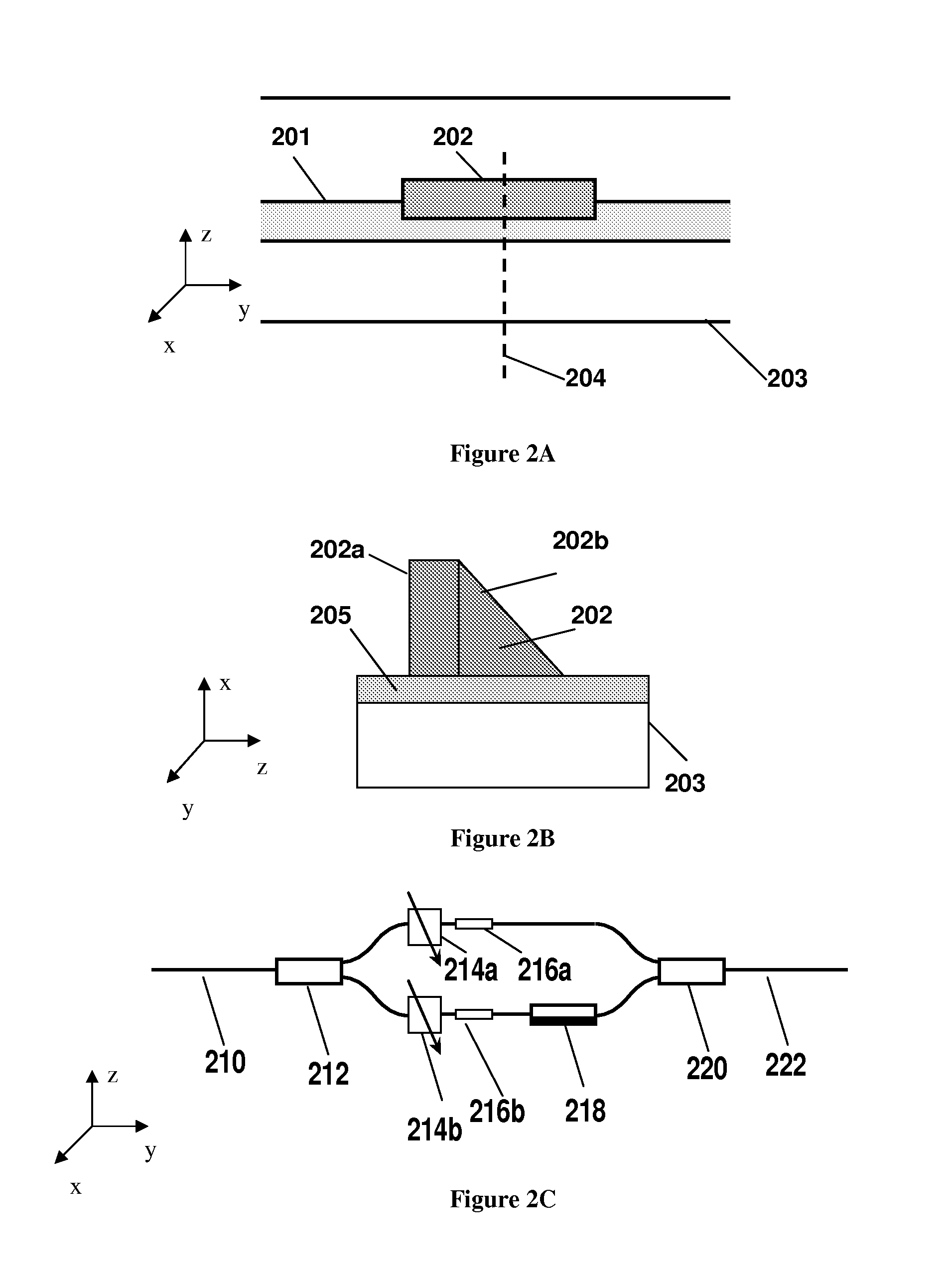
[0051]The embodiment illustrated in FIG. 5 includes many components and features that are similar to the components and features described in the embodiment illustrated in FIG. 3. For example, the embodiment illustrated in FIG. 5 comprises a LO 501, an optional optical amplifier section 502, a mixer 503 and a plurality of photodetectors 506. In various embodiments, the embodiment illustrated in FIG. 5 may include a mode converter 505 at the input interface. The embodiment illustrated in FIG. 5 further comprises a tunable polarization rotator 504 disposed between the output of the LO 501 and the input of the optical mixer 503. The tunable polarization rotator 504 may be similar to the various embodiments of the polarization rotator described with reference to FIGS. 2A-2C. The output of the tunable polarization rotator can be tuned to match the polarization of the optical signal generated by the LO 501 to the polarization of the incoming modulated optical signal coupled in to the devi...


PUM

PropertyMeasurementUnit
distanceaaaaaaaaaa
angleaaaaaaaaaa
angleaaaaaaaaaa

Abstract

Various embodiments of a coherent receiver including a widely tunable local oscillator laser are described herein. In some embodiments, the coherent receiver can be integrated with waveguides, optical splitters and detectors to form a monolithic optical hetero/homodyne receiver. In some embodiments, the coherent receiver can demodulate the full phase information in two polarizations of a received optical signal over a range of optical wavelengths.

Description

CROSS-REFERENCE TO RELATED APPLICATIONS[0001]This application claims the benefit under 35 U.S.C. §119(e) of U.S. Provisional Application 61 / 182,017 filed on May 28, 2009 titled “Chip-Based Advanced Modulation Format Transmitter,” which is hereby expressly incorporated herein by reference in its entirety.[0002]This application also claims the benefit under 35 U.S.C. §119(e) of U.S. Provisional Application 61 / 182,022 filed on May 28, 2009 titled “Monolithic Widely-Tunable Coherent Receiver,” which is hereby expressly incorporated herein by reference in its entirety.BACKGROUND OF THE INVENTION[0003]1. Field of the Invention[0004]Various embodiments of the invention relates to the area of optical communications photonic integrated circuits (PICs). In particular, the embodiments described herein generally relate to receivers for fiber optic or free space communications, and coherent receivers with monolithically integrated tunable local oscillator light sources.[0005]2. Description of th...

Claims


Application Information

Patent Timeline
Patent Type & Authority Applications(United States)
IPC IPC(8): H04B10/06G02B27/28B23P11/00
CPCH04B10/505H04B10/516H04B10/5161H04B10/615H04B10/6151H04B10/801G02F2001/212Y10T29/49826G02B2006/12104G02B6/2766G02B6/125G02F1/2257G02F1/2255H04B10/503G02F1/212
Inventor BARTON, JONATHONMASHANOVITCH, MILAN
Owner FREEDOM PHOTONICS LLC
Why Eureka
Try Eureka