Gas-phase functionalization of surfaces including carbon-based surfaces

a technology of functionalization and carbon-based surfaces, applied in the field of forming layers, can solve the problems of inability to guarantee the reproducibility or uniformity of mwnt ald coatings, and the inability to form mwnt ald coatings on the surface of these structures, and achieve continuous ald coating on a swnt by ald that is not in general conventionally achievable for any process condition

Inactive Publication Date: 2010-12-23
PRESIDENT & FELLOWS OF HARVARD COLLEGE
View PDF8 Cites 63 Cited by
  • Summary
  • Abstract
  • Description
  • Claims
  • Application Information

AI Technical Summary

Benefits of technology

[0016]This enables production of a single-walled carbon nanotube that is connected between electrically conducting source and drain contacts, with an insulating layer of a first thickness disposed on at least a portion of the source and drain contacts and covering a span of the nanotube, at each end of the nanotube at the source and drain contacts, that is substantially equal to the first thickness. Then a gate dielectric layer of a second thickness, less than the first thickness, can be disposed coaxially around a central span of the nanotube on which was not disposed the insulating layer of a first thickness, and an electrically conducting gate metal layer can be disposed at least coaxially around the dielectric layer on the nanotube.

Problems solved by technology

In the fabrication of electronic and microelectromechanical systems, a selected coating material or coating process can be found incompatible with a chosen substrate or material structure on which the coating material is to be formed.
As a result, many materials cannot be deposited or otherwise formed on the surfaces of these structures.
MWNT ALD coatings therefore cannot be guaranteed to be reproducible or uniform.
As a result, continuous ALD coating onto a SWNT by ALD is not in general conventionally achievable for any process conditions.
Other similar scenarios exist in which a selected coating material or coating process is found incompatible with a chosen nanotube wall structure or other configuration.
For example, chemical vapor deposition processes in general cannot be guaranteed to produce a uniform nanotube coaxial coating, and can require plasmas or deposition temperatures that are so high as to impact the electrical or mechanical properties of a nanotube.
For many process conditions, SWNTs are chemically inert to CVD precursors at CVD temperatures less than about 400° C. Although physical deposition methods (PVD), such as sputtering or evaporation, can sometimes deposit metals or other materials directly onto SWNTs, such deposits are not conformal, and do not uniformly surround the tubes due to, e.g., the directional nature of the methods.
It is therefore difficult to reliably and benignly make conformal layers of material around a nanotube.
But in general it can be difficult to uniformly and conformally coat a nanotube, and particularly a SWNT, with selected materials.
CVD and PVD techniques do not reliably produce a thin, uniform and conformal layer on a nanotube.
Liquid-chemical deposition methods are known to enable the coating of SWNTs with SiO2, which is a low-κ dielectric, but do not enable the deposition of higher-κ materials on a nanotube.
While this technique indeed enables uniform ALD film deposition on covalently functionalized SWNT surfaces, the liquid-based process is procedurally tedious and could be impractical for large-scale fabrication scenarios.
Furthermore, the covalent nature of the chemical bonding process can in general change the hybridization state of a nanotube, destroying optoelectronic and / or other properties of the nanotube.
As a result, it has heretofore been impractical to employ covalent functionalization as a means for enabling uniform deposition of a selected material, and particularly an insulating material, on a carbon nanotube.
Covalent functionalization of such carbon-based structures is for many applications detrimental and / or not possible within the limitations of a given microfabrication process sequence.
The technical potential for such structures in microelectronic and nanoscale system applications is therefore limited by an inability to form layers of selected materials on the structures.

Method used


Image

  • Gas-phase functionalization of surfaces including carbon-based surfaces
  • Gas-phase functionalization of surfaces including carbon-based surfaces
  • Gas-phase functionalization of surfaces including carbon-based surfaces

Examples


example i

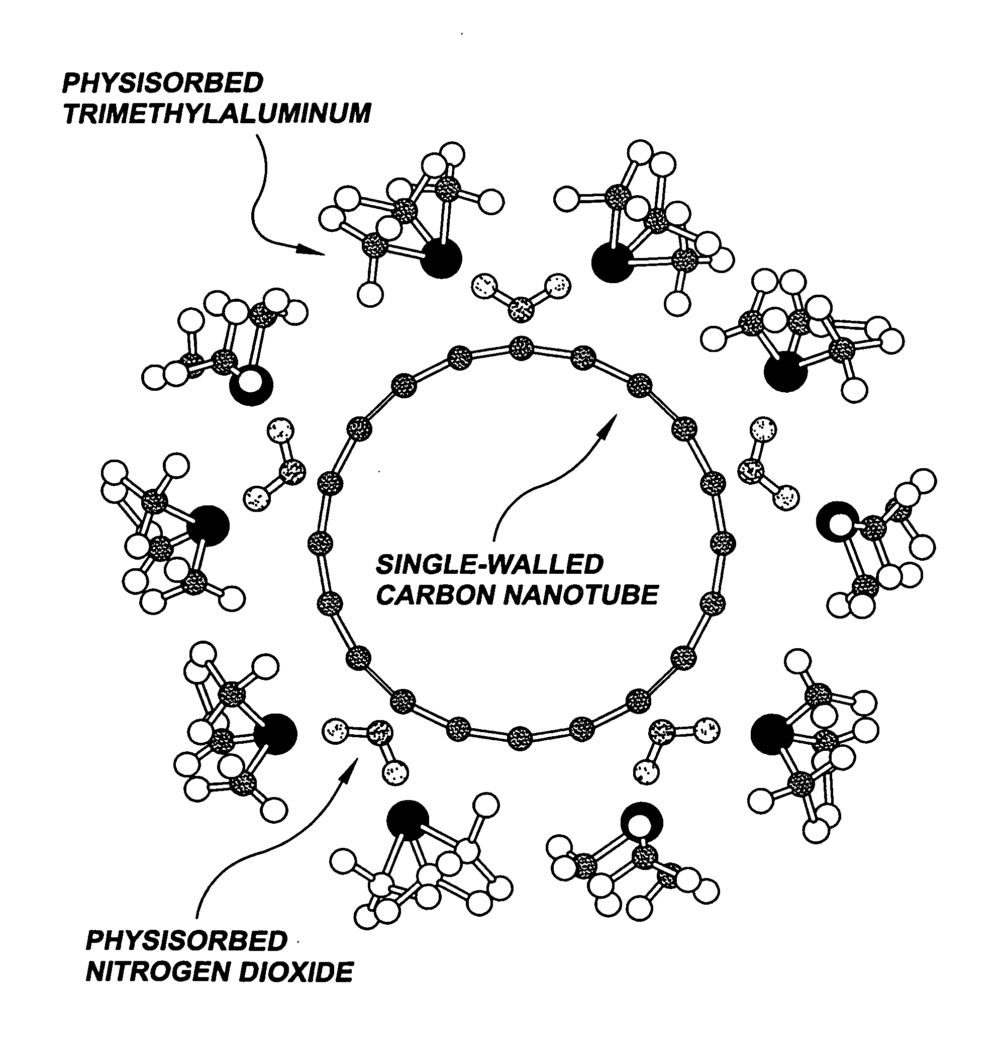
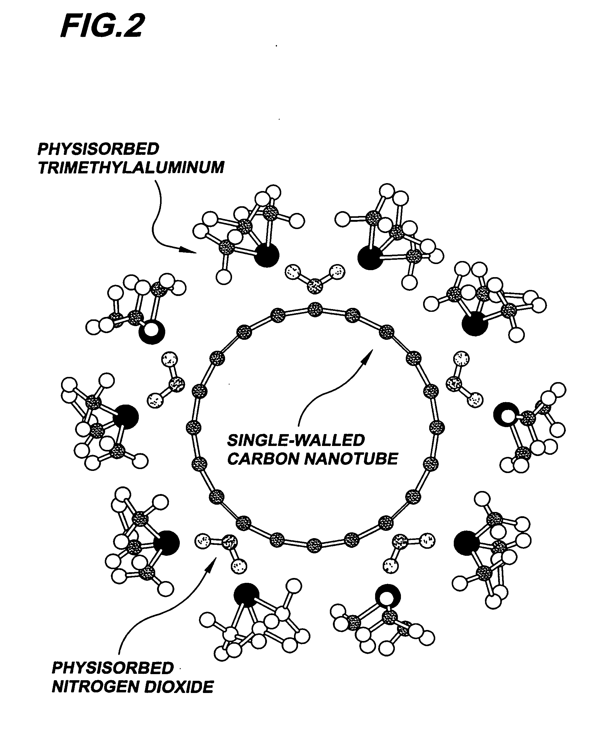
NO2 Adsorption and Desorption from a Carbon Nanotube

[0103]The electrical conductance of SWNTs was experimentally analyzed during the functionalization procedure of the invention. To produce structures for analysis, optical lithography and electron beam evaporation techniques were employed to pattern metal electrodes of 50 nm-thick Mo and 50 nm-thick Ti layers on quartz substrates. A focused ion beam (FIB) was employed to form trenches of 1 μm in width and 0.5 μm in depth between the edges of the metal electrodes. A layer of approximately 0.5 nm in thickness of Al2O3 was deposited by ALD on the electrode surfaces to prevent alloying between the molybdenum and the nanotube catalyst metal subsequently deposited. A catalyst region of Co of about 0.3 nm in thickness was deposited and patterned by liftoff on the electrode surfaces to form isolated catalyst regions.

[0104]SWNT synthesis was carried out at atmospheric pressure by bubbling argon at a flow rate of about 450 sccm through ethano...

example ii

TMA Stabilization of Adsorbed NO2

[0108]Suspended SWNTs were fabricated in the configuration of Example I and exposed to pulsed dosing of TMA. Here approximately 6 mL doses of TMA at a pressure of about 10 Torr were pulsed over suspended SWNTs under the same conditions that were used in the NO2 pulsing of Example I. During the pulsed dosing the conductance of the SWNTs was measured.

[0109]FIG. 3B is a plot of measured conductance of a SWNT as a function of time during pulsed TMA dosing. TMA exposure has an effect on the conductive properties of SWNTs that is the opposite of that due to NO2 exposure, and thus causes a decrease in SWNT conductance. The measured SWNT conductance following a TMA pulse exposure is seen in the plot to recover slightly due to desorption after each pulse, but it does not return to a constant baseline value as it did with NO2 exposure. This results in an overall negative slope in the conductance / time profile, which may be due to an increase in contact resista...

example iii

Functionalization Layer Thickness Control by ALD Cycle Number

[0113]SWNTs were synthesized as in Example I. The SWNTs were subjected to various NO2-TMA functionalization processes, with the number of NO2-TMA functionalization cycles adjusted to elucidate the nature of the resulting functionalization layer. For each process, a vacuum pressure of about 300 mTorr, under the continuous flow of argon at a flow rate of about 50 sccm, at a temperature of about 25° C., was employed. One functionalization cycle consisted of a 30 mL NO2 vapor dose at about 960 Torr followed by a 2 min purge with argon, then a 6 mL TMA vapor dose at about 10 Torr, followed by a 2 min purge. FIG. 4A is a plot of the thickness of the functionalization layer as a function of the number of NO2-TMA cycles.

[0114]As shown in the plot, the thickness of the functionalization layer remained constant at about one monolayer for up to about 100 NO2-TMA cycles. This preserved functionalization layer thickness within the firs...


PUM

PropertyMeasurementUnit
temperatureaaaaaaaaaa

Abstract

The invention provides methods functionalizing a planar surface of a graphene layer, a graphite surface, or microelectronic structure. The graphene layer, graphite surface, or planar microelectronic structure surface is exposed to at least one vapor including at least one functionalization species that non-covalently bonds to the graphene layer, a graphite surface, or planar microelectronic surface while providing a functionalization layer of chemically functional groups, to produce a functionalized graphene layer, graphite surface, or planar microelectronic surface.

Description

CROSS-REFERENCE TO RELATED APPLICATIONS[0001]This is a continuation-in-part of prior application Ser. No. 11 / 703,375, filed Feb. 7, 2007, which claims the benefit of U.S. Provisional Application No. 60 / 766,000, filed Feb. 7, 2006, the entirety of both of which applications are hereby incorporated by reference. This application claims the benefit of U.S. Provisional Application No. 60 / 934,454, filed Jun. 13, 2007, the entirety of which is hereby incorporated by reference.STATEMENT REGARDING FEDERALLY SPONSORED RESEARCH[0002]This invention was made with Government support under Contract No. CTS-0236584 awarded by NSF. The Government has certain rights in the invention.BACKGROUND OF THE INVENTION[0003]This invention relates to techniques for forming layers of material on a surface of a structure, and more particularly relates to techniques for functionalizing surfaces, including surfaces of carbon-based structures, to enable the formation of layers of material on a structure surface.[0...

Claims


Application Information

Patent Timeline
Patent Type & Authority Applications(United States)
IPC IPC(8): H01L29/775B05D5/12B32B9/00H01L21/30C01F7/304
CPCB82Y10/00Y10T428/2918B82Y40/00C01B31/0273C01B2202/02C01F7/304C01P2004/13H01L51/0049H01L51/057H01L51/0595Y10S977/89Y10S977/755Y10S977/734Y10S977/842Y10S977/847B82Y30/00C01B32/174H10K85/225H10K10/491H10K10/701
Inventor GORDON, ROY G.FARMER, DAMON B.
Owner PRESIDENT & FELLOWS OF HARVARD COLLEGE
Why Eureka
Try Eureka