Phase shift mask blank and phase shift mask

a phase shift mask and mask technology, applied in the field of phase shift mask blank and phase shift mask, can solve the problems of no optimization, pattern collapsing, etc., and the thickness of the photomask is reduced, and the over etching time is reduced, and the thickness of the light-shielding film is reduced. , the effect of reducing the thickness of the light-shielding film

Active Publication Date: 2011-05-12
HOYA CORP
View PDF5 Cites 20 Cited by
  • Summary
  • Abstract
  • Description
  • Claims
  • Application Information

AI Technical Summary

Benefits of technology

[0065]It is possible to reduce the thickness of a light-shielding film of a phase shift mask blank in a preferred embodiment of the present invention, and this enables reduction in clear etching time (CET), and in addition, over etching time (OET) is also reduced. In particular, in a photomask blank in a preferred embodiment of the present invention, it is possible to reduce the thickness of a light-shielding film having a structure made of a plurality of layers (particularly a three-layer structure) by providing a light-shielding layer (absorption layer) having a high content of a metal such as Cr, and this enables reduction in clear etching time (CET) and over etching time (OET).
[0066]Moreover, in a phase shift mask blank in a preferred embodiment of the present invention, over etching time (OET) can be reduced by combining a film containing a metal (e.g., Cr) having a high etching rate (ER) (antireflection layer) with a metal-containing film having a low etching rate (ER) (absorption layer), by providing a predetermined balance between the thickness of the layer having the high etching rate (ER) and the thickness of the layer having the low etching rate (ER), and by disposing the layer having the low etching rate (ER) at a predetermined position.
[0067]In a phase shift mask blank in a preferred embodiment of the present invention, the thickness of a resist formed on a light-shielding film can be reduced by reducing clear etching time (CET), over etching time (OET) or both of them. As a result, in the phase shift mask blank in the preferred embodiment of the present invention, the problem of pattern collapsing, etc. is not easily caused, and therefore, a fine mask pattern can be formed thereby.
[0068]Moreover, in a preferred embodiment of the present invention, by providing a structure in which a plurality of layers having a different metal content with a predetermined thickness are laminated, it is possible to provide a phase shift mask blank comprising a light-shielding film having a predetermined thickness by which a sufficient optical density can be provided, wherein the etching rate (ER) of the entire light-shielding film is high.

Problems solved by technology

However, when the resist film thickness is increased, the aspect ratio is increased, and this causes the problem of pattern collapsing, etc., particularly in the case where a fine pattern is to be formed.
However, regarding the above-described CrON film, it is just that the optical density per unit film thickness at a wavelength of 450 nm is set, and regarding a wavelength of exposure light equal to or less than wave length of an ArF excimer laser light, no optimization has been made.
In particular, in the case of hyper-NA lithography, the angle of light incidence relative to a photomask becomes shallower, and this causes the problem that a miniaturized mask pattern itself shades a transfer image (shadowing).
In addition, the cross-section shape is prone to vary, and this, together with shadowing, causes reduction of transfer accuracy of CD (Critical Dimension).

Method used


Image

  • Phase shift mask blank and phase shift mask
  • Phase shift mask blank and phase shift mask
  • Phase shift mask blank and phase shift mask

Examples


first embodiment

1. First Embodiment

[0078]At the time of processing a light-shielding film formed on a phase shift film, the present inventor found the following matters:[0079](1) in the case of a two-layer structure made of a light-shielding layer and a front-surface antireflection layer, when the light-shielding layer that is a lower layer is formed with a material having a low etching rate, longer over etching time is required, and as a result, the total etching time is increased, whereas when the lower layer is formed with a material having a high etching rate, clear etching time is reduced, but there is a case where over etching time is increased due to loading, and thus, it is difficult to reduce etching time when using the two-layer structure; and[0080](2) in order to reduce over etching time, it is preferred to employ a three-layer structure consisting of a lower layer, an interlayer and an upper layer, wherein a material having an etching rate higher than that of the interlayer is used for ...

second embodiment

2. Second Embodiment

[0130](1) The phase shift mask blank of the second embodiment is as follows:[0131]the phase shift mask blank of the present invention, which is an original plate of a phase shift mask exposed to an ArF excimer laser light, wherein:

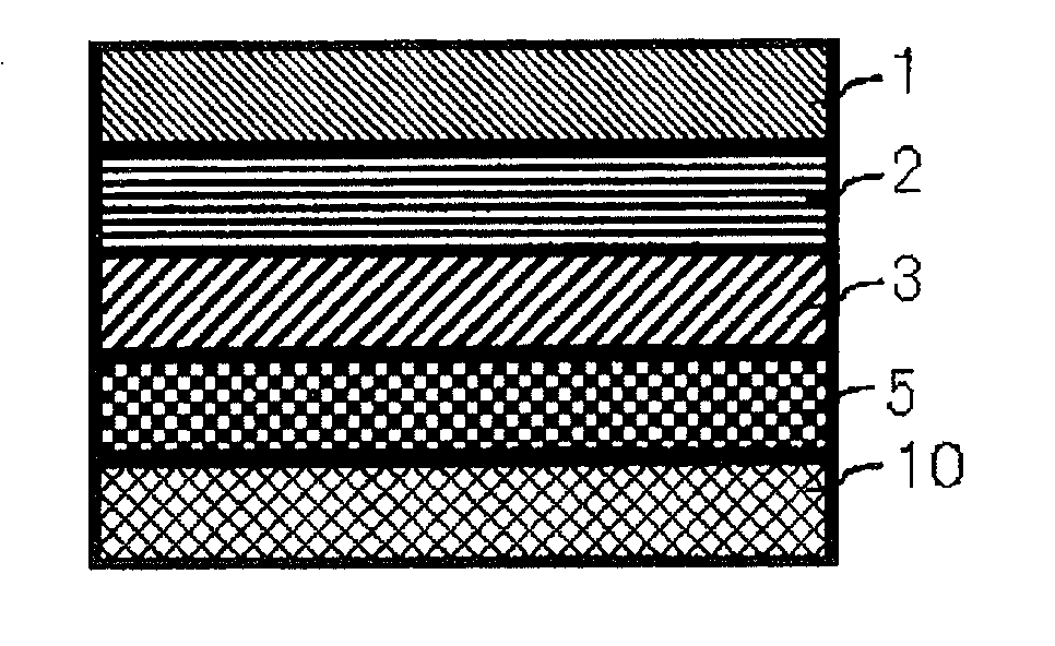
[0132]the phase shift mask blank has a light transmissive substrate, a phase shift film and a light-shielding film;

[0133]the phase shift film is provided between the light transmissive substrate and the light-shielding film;

[0134]the light-shielding film consists of a plurality of layers;

[0135]the optical density of the entire light-shielding film is 1.8 to 2.6;

[0136]the ratio of the optical density of a layer A constituting the plurality of layers to the sum of the optical densities of all the layers other than the layer A is 1:5 to 1:19;

[0137]each of the layers constituting the light-shielding film contains a metal; and

[0138]the layers other than the layer A consist of a film comprising: the same metal as that contained in the layer A...

third embodiment

3. Third Embodiment

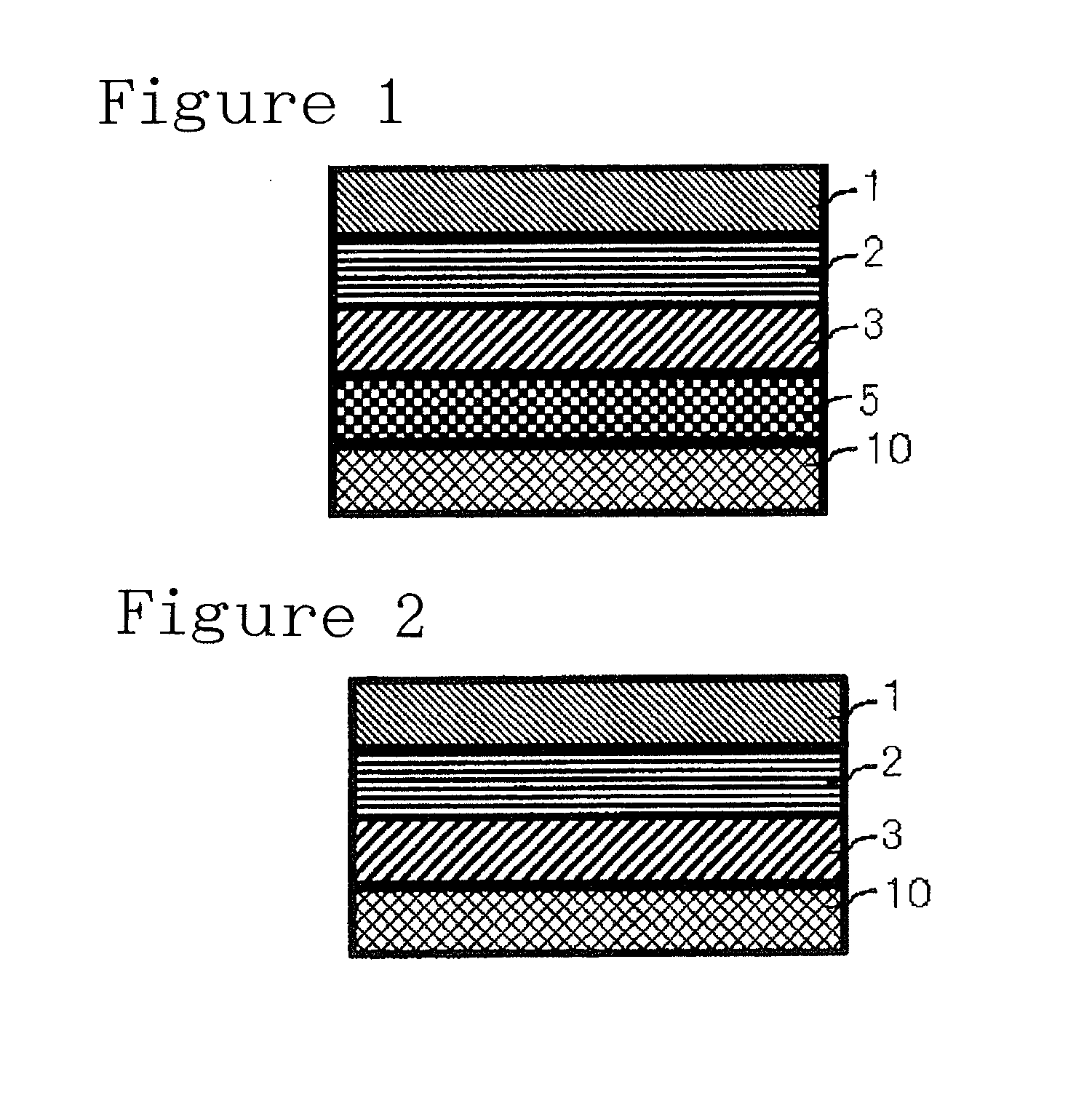
[0161](1) The phase shift mask blank of the third embodiment is as follows:[0162]the phase shift mask blank of the present invention, which is an original plate of a phase shift mask exposed to an ArF excimer laser light, wherein:

[0163]the phase shift mask blank has a light transmissive substrate, a phase shift film and a light-shielding film;

[0164]the phase shift film is provided between the light transmissive substrate and the light-shielding film;

[0165]the light-shielding film has a laminated structure in which a lower layer, an interlayer and an upper layer are laminated in this order from the side close to the light transmissive substrate;

[0166]the lower layer is made of a CrOCN film, which is formed using Cr as a target in a mixed gas atmosphere comprising 45 to 65 vol % of an inert gas, 30 to 50 vol % of CO2 gas and 1 to 15 vol % of N2 gas;

[0167]the interlayer is made of a CrN film, which is formed using Cr as a target in a mixed gas atmosphere comprising 7...


PUM

PropertyMeasurementUnit
transmittanceaaaaaaaaaa
thicknessaaaaaaaaaa
transmittanceaaaaaaaaaa

Abstract

The present invention provides a photomask blank used for producing a photomask to which an ArF excimer laser light is applied, wherein: a light-shielding film is provided on a light transmissive substrate; the light-shielding film has a laminated structure in which a lower layer, an interlayer and an upper layer are laminated in this order from the side close to the light transmissive substrate; the thickness of the entire light-shielding film is 60 nm or less; the lower layer is made of a film containing a metal and has a first etching rate; the upper layer is made of a film containing a metal and has a third etching rate; the interlayer is made of a film containing the same metal as that contained in the lower layer or the upper layer and has a second etching rate that is lower than the first etching rate and the third etching rate; and the thickness of the interlayer is 30% or less of the thickness of the entire light-shielding film.

Description

TECHNICAL FIELD[0001]The present invention relates to a phase shift mask blank and a phase shift mask.BACKGROUND ART[0002]In general, in the production processes of high-density semiconductor integrated circuits such as LSI, color filters for CCD (charge-coupled device) and LCD (liquid crystal display device), magnetic heads, etc., microfabrication utilizing the photolithographic technique using photomasks is performed.[0003]In this microfabrication, a photomask, in which a light-shielding film consisting of a metal thin film such as a chromium film is generally formed on a light transmissive substrate made of quartz glass, aluminosilicate glass or the like by means of sputtering, vacuum deposition or the like to provide a photomask blank, wherein the light-shielding film is formed to have a predetermined pattern, is used.[0004]A photomask is produced using such a photomask blank with the following processes: an exposure process in which a desired pattern exposure is applied to a re...

Claims


Application Information

Patent Timeline
Patent Type & Authority Applications(United States)
IPC IPC(8): G03F1/00
CPCG03F1/14G03F1/58G03F1/32G03F1/26H01L21/0274H01L21/0337G03F1/62
Inventor IWASHITA, HIROYUKISHISHIDO, HIROAKIKOMINATO, ATSUSHIHASHIMOTO, MASAHIRO
Owner HOYA CORP
Why Eureka
Try Eureka