Photoelectric conversion device

Inactive Publication Date: 2011-05-26
MITSUBISHI HEAVY IND LTD
View PDF2 Cites 4 Cited by
  • Summary
  • Abstract
  • Description
  • Claims
  • Application Information

AI Technical Summary

Benefits of technology

[0021]When the intermediate contact layer mainly containing a compound represented by Zn1-xMgxO (0.096≦x≦0.183) is formed between the adjacent power generation cell layers, it is possible to suppress the leakage current in the cell-connected portion and to reduce the contact resistance in the film vertical direction. Therefore, the form factor is improved, thus realizing a photoelectric conversion device having hi

Problems solved by technology

However, thin-film silicon solar cells have the disadvantage that the conversion efficiency thereof is lower than that of crystalline solar cells.
In this technical field, an improvement in the conversion efficiency is a key issue, and a tandem solar cell having a photoelectric conversion layer in which two power generation cell layers

Method used


Image

  • Photoelectric conversion device
  • Photoelectric conversion device
  • Photoelectric conversion device

Examples


first embodiment

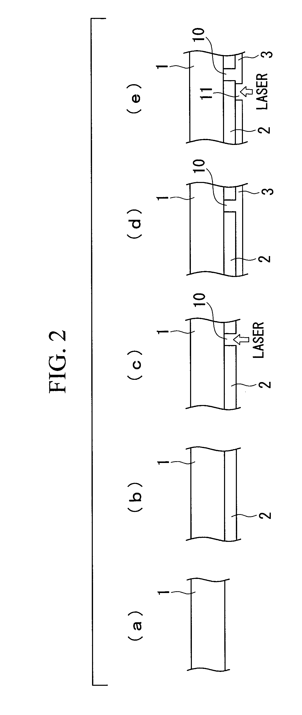
[0034]A method for fabricating a photoelectric conversion device according to a first embodiment will be described by using, as an example, the steps for fabricating a solar cell panel. FIGS. 2 to 5 are views showing, in outline, a method for fabricating a solar cell panel of this embodiment.

(1) FIG. 2(a)

[0035]As the substrate 1, a soda float glass substrate (with a substrate area of 1 m square or more, for example, 1.4 m×1.1 m×plate thickness: 3.5 mm to 4.5 mm) is used. It is preferable that end faces of the substrate be subjected to a corner chamfering process or an R-chamfering process in order to avoid damage caused by thermal stress, impacts, or the like.

(2) FIG. 2(b)

[0036]As the transparent electrode layer 2, a transparent electrode film composed mainly of tin oxide (SnO2) and having a film thickness of about 500 nm to 800 nm, inclusive, is formed at about 500° C. using a thermal CVD apparatus. At this time, a suitable uneven texture is formed on the surface of the transparent...

second embodiment

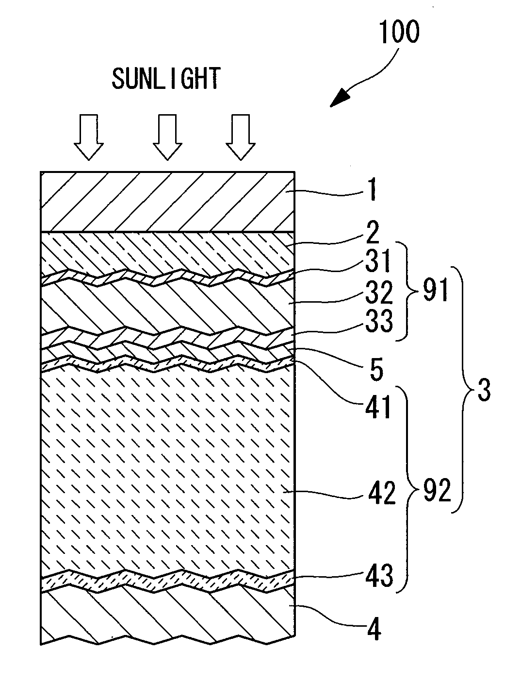
[0064]A photoelectric conversion device according to a second embodiment includes an interfacial layer between the first power generation cell layer 91 and the intermediate contact layer 5, shown in FIG. 1.

[0065]The interfacial layer mainly contains ZnO or a compound represented by Zn1-xMgxO(where 01-xMgxO used as the interfacial layer may contain Ga2O3 as a dopant.

[0066]The interfacial layer may be formed in a film-forming chamber different from or identical to that is used to form the intermediate contact layer.

[0067]When the interfacial layer and the intermediate contact layer are formed in different film-forming chambers, the interfacial layer and the intermediate contact layer are formed by the following steps.

[0068]The interfacial layer is formed, using an RF magnetron sputtering apparatus, under the following conditions: a Ga2O3-doped ZnO sintered compact or a Ga2O3-doped ZnO—MgO mixture target (MgO ratio: 0 to 5 mass %, excluding 0 mass %), an RF power of 1.1 to 4.4 W / cm2, a...

example 1

[0073]A tandem solar cell module having the structure shown in FIG. 1 was formed on a glass substrate (5 cm square). Note that the film thickness of the i-layer of the first power generation cell layer was 250 nm, and the film thickness of the i-layer of the second power generation cell layer was 1.9 μm.

[0074]The intermediate contact layer was formed under the following conditions: a ZnO sintered compact target (Ga2O3 dopant) or a ZnO—MgO mixture target (Ga2O3 dopant, MgO mass ratio: 5 to 12.5%), a substrate temperature of 25° C., an RF power of 4.4 W / cm2, a target-to-substrate distance of 90 mm, a film-formation speed of 0.17 nm / s, and a film thickness of 70 nm.

[0075]FIG. 7 shows the relationship between the MgO content in the intermediate contact layer and the module form factor. In the figure, the horizontal axis shows the MgO content, and the vertical axis shows the module form factor normalized by a value when the MgO content was 0%. FIG. 8 shows the relationship between the Mg...


PUM

PropertyMeasurementUnit
Thicknessaaaaaaaaaa
Thicknessaaaaaaaaaa
Electrical resistanceaaaaaaaaaa

Abstract

Provided is a photoelectric conversion device in which the conductivity after hydrogen-plasma exposure is set within an appropriate range, thereby suppressing the leakage current and improving the conversion efficiency. A photoelectric conversion device includes, on a substrate, a photoelectric conversion layer having at least two power generation cell layers, and an intermediate contact layer provided between the power generation cell layers. The intermediate contact layer mainly contains a compound represented by Zn1-xMgxO (0.096≦x≦0.183).

Description

RELATED APPLICATIONS[0001]The present application is a U.S. National Phase of International Application Number PCT / JP2009 / 064570, filed Aug. 20, 2009, and claims priority from Japanese Application Number 2008-295750, filed Nov. 19, 2008.TECHNICAL FIELD[0002]The present invention relates to solar cells and in particular, to a thin-film solar cell fabricated by forming power generation layers.BACKGROUND ART[0003]As a photoelectric conversion device used for a solar cell that converts the energy in sunlight into electrical energy, there is a known thin-film silicon photoelectric conversion device having a photoelectric conversion layer fabricated by forming thin films of a p-type silicon semiconductor (p-layer), an i-type silicon semiconductor (i-layer), and an n-type silicon semiconductor (n-layer) by using a plasma CVD method or the like.[0004]Thin-film silicon solar cells have the advantages that the area thereof can be easily increased, and only a small amount of material is used b...

Claims


Application Information

Patent Timeline
IPC IPC(8): H01L31/042
CPCB23K26/063H01L31/0547B23K26/36B23K26/367B23K26/4075B23K2201/40C23C14/086C23C14/3407H01L31/022466H01L31/0687H01L31/076H01L31/1884Y02E10/52Y02E10/544Y02E10/548B23K26/0853B23K26/364B23K26/0622B23K26/40H01L31/022483B23K2101/40B23K2103/50H01L31/04
Inventor YAMAGUCHI, KENGOSAKAI, SATOSHITSURUGA, SHIGENORI
Owner MITSUBISHI HEAVY IND LTD
Why Eureka
Try Eureka