Wafer polishing method and double-side polishing apparatus

a polishing method and polishing technology, applied in the direction of manufacturing tools, semiconductor/solid-state device testing/measurement, lapping machines, etc., can solve the problems of failure in the shape of the wafer, thereby occurring, and productivity decline, etc., to achieve high flatness, high precision, and easy to obtain

Active Publication Date: 2011-06-02
SHIN-ETSU HANDOTAI CO LTD
View PDF17 Cites 37 Cited by
  • Summary
  • Abstract
  • Description
  • Claims
  • Application Information

AI Technical Summary

Benefits of technology

[0073]The wafer having a high flatness can be consequently readily obtained while measuring the thickness of the wafer with high precision.
[0074]As explained above, the wafer polishing method according to the present invention enables the improvement in the deterioration of the shape of the wafer, such as the outer peripheral sag, due to small changes of the polishing conditions during polishing, the changes which are accompanied by the deterioration of the polishing jig material such as the polishing pad and the carrier, and the stabilization of the flatness of each wafer can be obtained.
[0075]In addition to these, since the polishing is performed while measuring the thickness of the wafer, the timing of the switching of the polishing agent can be changed on the basis of the deterioration of the polishing jig material such as the polishing pad and the carrier, and the target amount of the polishing stock removal can be obtained in relatively short time. The productivity can be therefore improved, the variation of the thickness can be made very small, and the yield can be greatly improved.
[0076]Moreover, the present invention provides the double-side polishing apparatus polishing while measuring the thickness of the wafer, the apparatus which can perform polishing while measuring the thickness of the wafer with high precision without being influenced by a measurement error as represented by the vibration of the wafer during polishing, does not have a particular waste, has a low running cost, can readily carry out the maintenance, and can polish while measuring the thickness of the wafer with high precision.

Problems solved by technology

In this method, however, the polishing conditions are not switched with taking account of deterioration of a polishing jig material such as the polishing pad and the carrier.
A failure in a wafer shape, such as an outer peripheral sag, thereby occurs.
Moreover, since timing of switching the polishing conditions is constant regardless of the deterioration of the polishing jig material such as the polishing pad and the carrier, there arise problems such that the productivity becomes worse by increasing a polishing time with the deterioration of the polishing pad, and that excess or deficiency of polishing stock removal occurs.
However, since the polishing needs to be stopped halfway and thereby the productivity becomes significantly worse, it is not realistic method.

Method used


Image

  • Wafer polishing method and double-side polishing apparatus
  • Wafer polishing method and double-side polishing apparatus
  • Wafer polishing method and double-side polishing apparatus

Examples


example 1

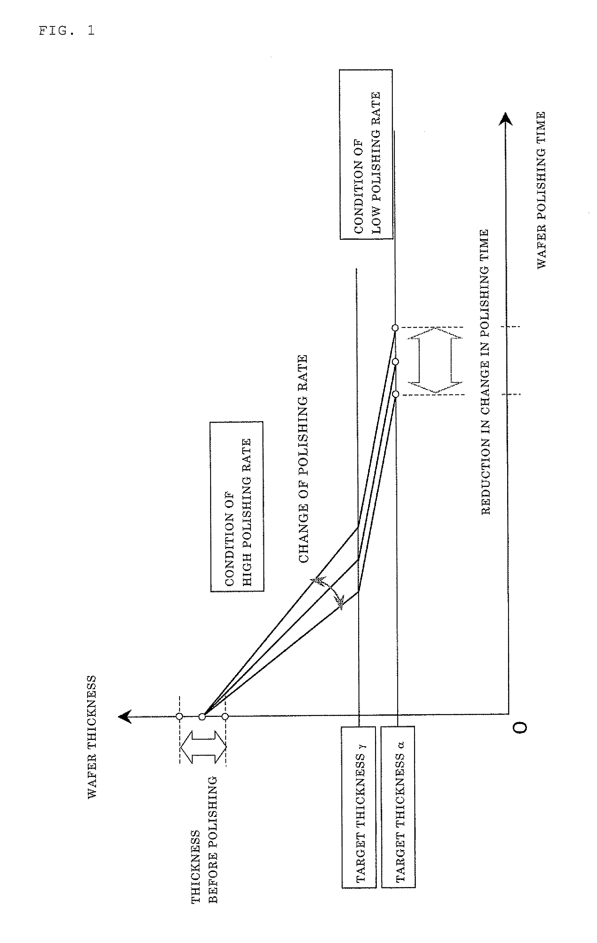
[0165]A wafer was polished according to the wafer polishing method as shown in FIG. 1.

[0166]As the wafer to be polished, there were prepared 720 silicon single wafers having a diameter of 300 mm and p−-type obtained by slicing, with a wire saw, an ingot grown by the CZ method. This p−-type wafer means a p-type wafer having a high resistivity. The wafers were subjected to chamfering, rapping, and etching in a normal condition.

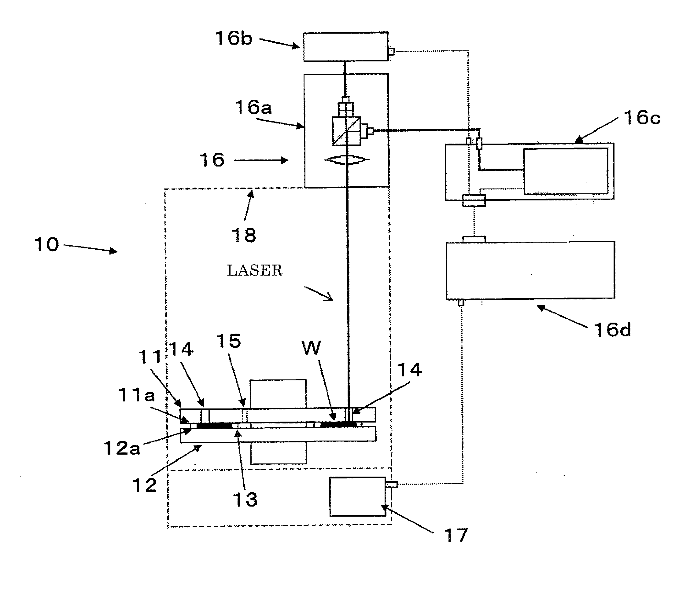
[0167]With the double-side polishing apparatus as shown in FIG. 7, 240 wafers of the prepared silicon single wafers were double-side polished in a batch-wise manner (15 wafers in one batch). As the polishing pad, MH-S15A of Nitta haas was used. As the polishing slurry before the switching, Fujimi FGL11022 (for the high rate polishing) was used, and as the polishing slurry after the switching, Fujimi FGL2100 (for the low rate polishing) was used. It is to be noted that an attempt to keep the thicknesses of all polished wafers constant was made.

[0168]In this case,...

example 2

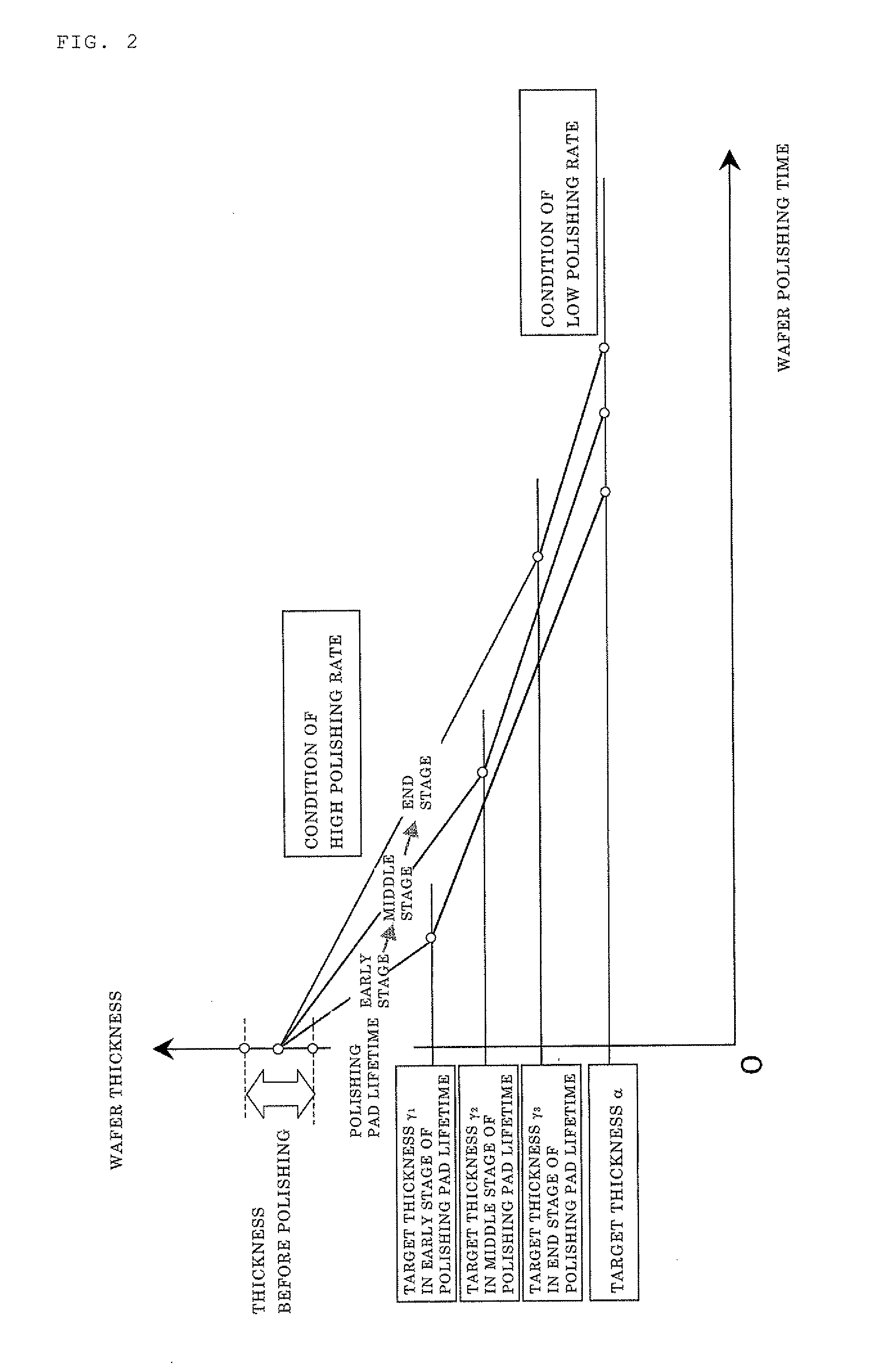
[0180]The double-side polishing apparatus as shown in FIG. 7 was used to polish the wafers in a batch-wise manner (15 wafers in one batch). In this case, the target thickness of each of the polished wafers was 777 μm.

[0181]As the wafer to be polished, there were prepared 600 silicon single wafers having a diameter of 300 mm and p−-type obtained by slicing, with a wire saw, an ingot grown by the CZ method. The wafers were subjected to chamfering, lapping, and etching. This p−-type wafer means a p-type wafer having a high resistivity.

[0182]There was prepared the wafer-thickness-measuring mechanism provided with the optical unit using the apparatus of a wavelength-variable-infrared laser, the apparatus which can tune the wavelength of the laser to 1575 to 1775 nm. With this wafer-thickness-measuring mechanism, 300 wafers of 600 wafers were polished while measuring the thickness of the wafer, and the thickness of each of the polished wafers was evaluated by AFS (a capacitance flatness-m...

example 3

[0188]The double-side polishing apparatus as shown in FIG. 10 was prepared.

[0189]First, 15 openings having a diameter of 20 mm were provided on the circumference of a circle where the center of the upper turn table is a fulcrum, as the plurality of openings. The polishing pad (polishing pad MH made by Nitta Naas co., a thickness of 1500 μm) having the holes having a diameter of 20 mm larger than that of an outer circumferential portion of each of the openings (a diameter of 40 mm) was prepared. The same number of the window members as the openings were also prepared, each window member in which PTS films made by toray co., (a diameter of 30 mm, a thickness of 150 μm) having a diameter of 10 mm larger than that of each of the openings provided at the turn table were cut into the shape of a circular disk, and adhesive double coated tapes (sumitomo 3M 442JS3, a thickness of 110 μm) were adhered along the outer circumference of the PTS films. The window members were adhered to portions ...


PUM


Abstract

The present invention is a wafer polishing method including simultaneously polishing both surfaces of a wafer by pressing and rubbing the wafer, while holding the wafer with: a lower turn table having a flat polishing-upper-surface rotationally driven; an upper turn table having a flat polishing-lower-surface rotationally driven, the upper turn table being arranged with facing to the lower turn table; and a carrier having a wafer-holding hole for holding the wafer, wherein the polishing is performed while measuring a thickness of the wafer through a plurality of openings provided between a rotation center and an edge of the upper turn table or the lower turn table, and switching a polishing slurry with a polishing slurry having a different polishing rate during the polishing of the wafer. As a result, there is provided a wafer polishing method that can manufacture a wafer having a high flatness and a high smoothness at high productivity and high yield.

Description

TECHNICAL FIELD[0001]The present invention relates to a wafer polishing method and a double-side polishing apparatus, and specifically to a wafer polishing method and a double-side polishing apparatus that can efficiently manufacture a wafer for a semiconductor having a high flatness.BACKGROUND ART[0002]A conventional wafer manufacturing method will be explained by an example of a silicon wafer manufacturing method. First, a silicon single crystal ingot is grown, for example, by the Czochralski method (the CZ method). The obtained silicon single crystal ingot is sliced to produce silicon wafers, and thereafter the silicon wafers are subjected to each of the steps of chamfering, lapping, and etching one after the other. At least a polishing process is subsequently performed to make a main surface of each wafer a mirror surface.[0003]In this polishing process of the wafer, for example, a double-side polishing apparatus may be used to polish both surfaces of the silicon wafer.[0004]As ...

Claims


Application Information

Patent Timeline
Patent Type & Authority Applications(United States)
IPC IPC(8): B24B49/12B24B37/04
CPCB24B37/042B24B37/08B24B49/12B24D7/12H01L21/02024H01L22/12H01L22/26H01L2924/0002B24B37/013B24B49/04H01L21/304H01L2924/00B24B37/00
Inventor FURUKAWA, DAISUKEASAI, KAZUMASAKIDA, TAKAHIROTANAKA, TADAO
Owner SHIN-ETSU HANDOTAI CO LTD
Why Eureka
Try Eureka