

Structure and method for making low leakage and low mismatch nmosfet
a technology of low leakage and low mismatch, applied in the direction of transistors, electrical apparatus, semiconductor devices, etc., can solve the problems of increasing chip power consumption, increasing cooling and packaging costs, and reducing performance, so as to increase the threshold voltage of each low leakage n
- Summary
- Abstract
- Description
- Claims
- Application Information
AI Technical Summary
Benefits of technology
Problems solved by technology
Method used
Image

Examples
Embodiment Construction
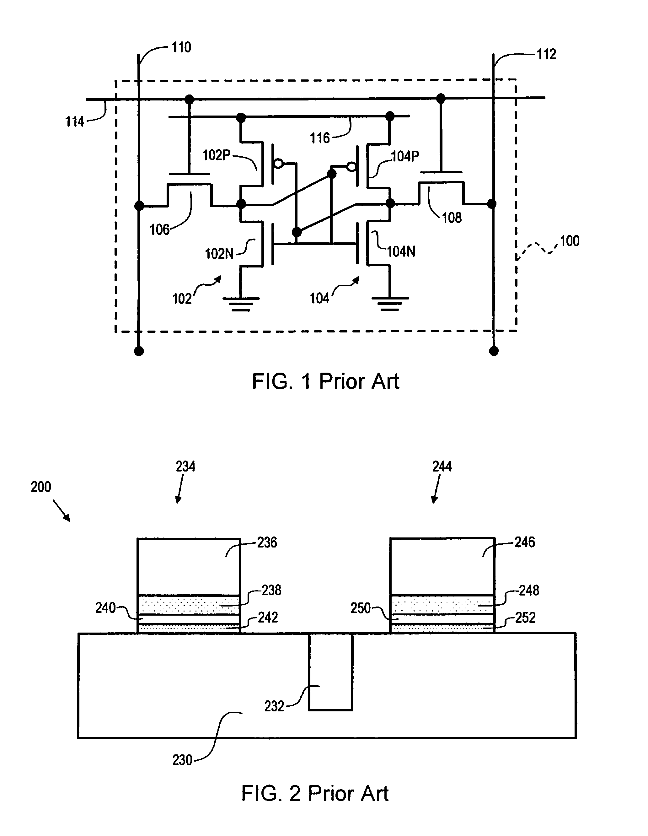
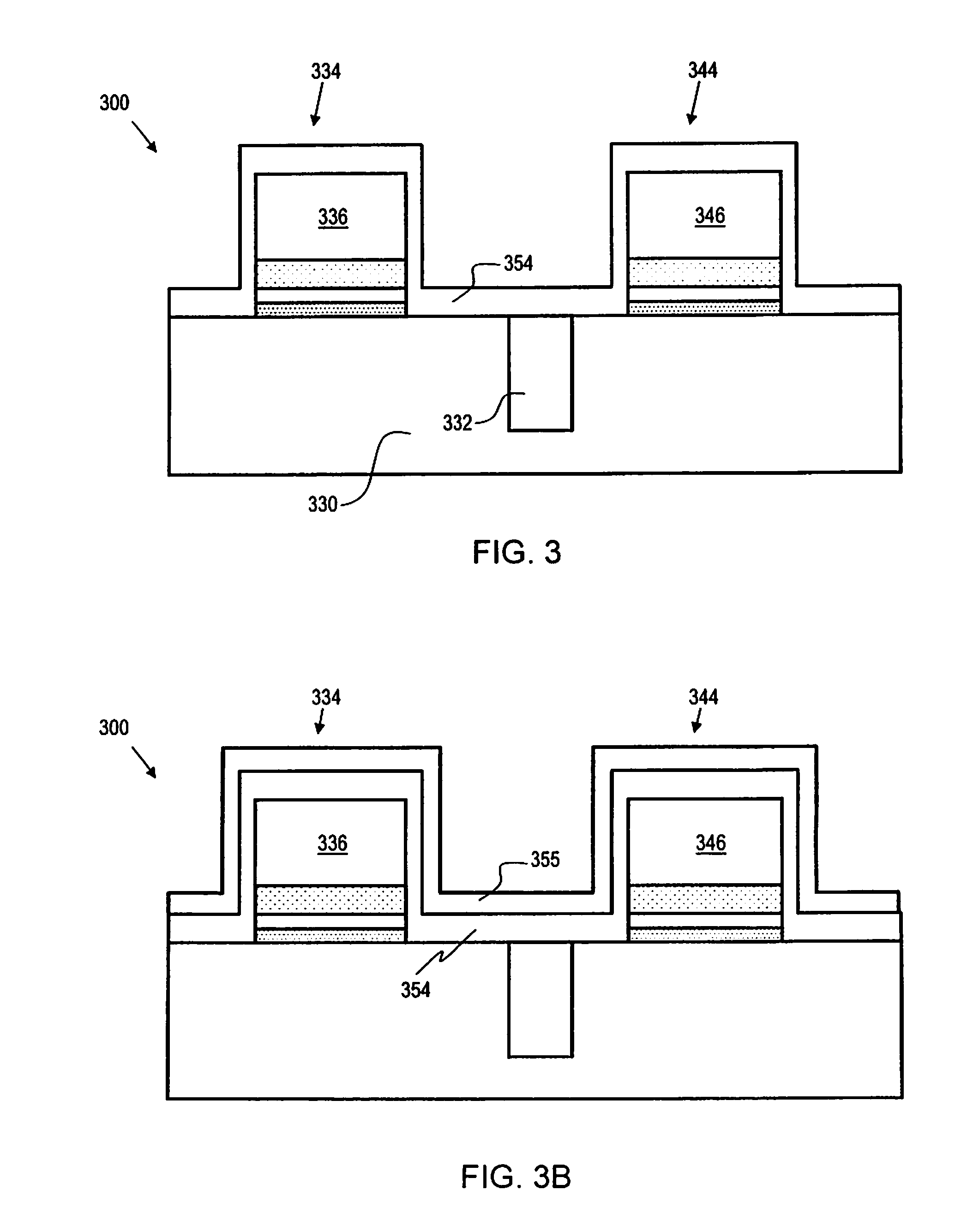
[0046]The present invention utilizes oxygen diffusion into a high-K metal gate stack to increase the effective gate oxide thickness and change metal gate effective work function. Using the process disclosed herein, oxygen diffusion only occurs on selected transistors, namely the NFETs that are used in situations where low leakage is an important factor. One such example is that of the NFET transistors that comprise SRAM cells. PFETs, and other NFETs (e.g. for logic purposes) do not have their gate stacks diffused with oxygen. Therefore, the SRAM NFETs are optimized for low leakage, whereas the other transistors (PFETs and logic NFET transistors) are not affected, due to the process steps disclosed herein. While the detailed description discusses embodiments of the present invention that pertain to SRAMS, other embodiments of the present invention can be applied to any circuit where a combination of logic NFETs, low leakage NFETs, and PFETs is desired. Embodiments of the present inve...
PUM
 Abstract
Description
Claims
Application Information