Transition Metal Ion Doped Semiconductor Nanocrystals and a Process for the Preparation Thereof

Inactive Publication Date: 2011-08-04
INDIAN ASSOC FOR THE CULTIVATION OF SCI
View PDF7 Cites 2 Cited by
  • Summary
  • Abstract
  • Description
  • Claims
  • Application Information

AI Technical Summary

Benefits of technology

[0013]Another object of the present invention is to provide free-flowing, transition metal ions doped semiconductor nanocrystals of high quantum yield in excess of 20% in both aqueous and non-aqueous media.
[0014]A furt

Problems solved by technology

In spite of their improved properties, these materials are not readily and widely accepted by the biological community because of the adverse toxicity of cadmium.
This paper also reports Mn doped ZnSe nanocrystals with about 50% quantum yield, but the task of generating stable and acceptable intensity emission nanocrystals and method of making them continued to remain a real challenge for the scientists for a considerable period of time, this material achieved still remains unacceptable since it contains selenium as a partially toxic material.
The main drawback of this synthesis process is that the raw materials include toxic phosphine chemicals.
However, the process includes use of organometallic precursors, which are toxic and explosive.
The synthesis method

Method used


Image

  • Transition Metal Ion Doped Semiconductor Nanocrystals and a Process for the Preparation Thereof
  • Transition Metal Ion Doped Semiconductor Nanocrystals and a Process for the Preparation Thereof
  • Transition Metal Ion Doped Semiconductor Nanocrystals and a Process for the Preparation Thereof

Examples


Example

Example 1

Process for the Preparation of Transition Metal Ion Doped Semiconductor Nanocrystals

[0077]Transition metal oxide stock solutions were prepared by taking 0.5 mmol of their respective acetates in 5 ml of oleylamine. The mixture was degassed and heated to get a clear solution. For Mn doped zinc sulfide nanocrystals first the host ZnS nanocrystals were synthesized and MnO solutions were injected during growth stage. For ZnS nanocrystals synthesis, 0.1 mmol of Zinc Stearate, Zn(St)2 and 10 ml of ODE are loaded in a 50 ml three necked flask, degassed for 10 minutes at 100° C. by purging with argon and then heated to 300° C. In a vial, 0.5 mmol S powder in 1 ml of ODE was taken with 0.3 g of ODA under argon and mixture was injected into the above reaction flask at 300° C. The temperature was reduced to 250° C. and 1 ml of MnO stock solution was injected. Then the reaction temperature was again increased to 280° C. for ZnS growth. 1.0 mmol Zn(St)2 with 0.5 mmol SA in 5 ml of ODE wa...

Example

Example 2

Process for the Estimation of Quantum Yield of the Transition Metal Ion Doped Semiconductor Nanocrystals at Aqueous and Non-Aqueous Medium

[0078]The QY of the nanocrystals were determined with respect to an organic dye named as Quinine sulphate.[0079]i. First absorption and emission of quinine sulphate was measured. The emission measurement was done at the excitation wavelength same to the doped nanocrystals.[0080]ii. Same procedure was applied for D-dots.

[0081]The emission area of both dye and d-dots were calculated. These emission areas were divided by their optical density (OD) value. The QY was calculated using a known formula. Quantum yield was increased by optimizing the reaction condition.

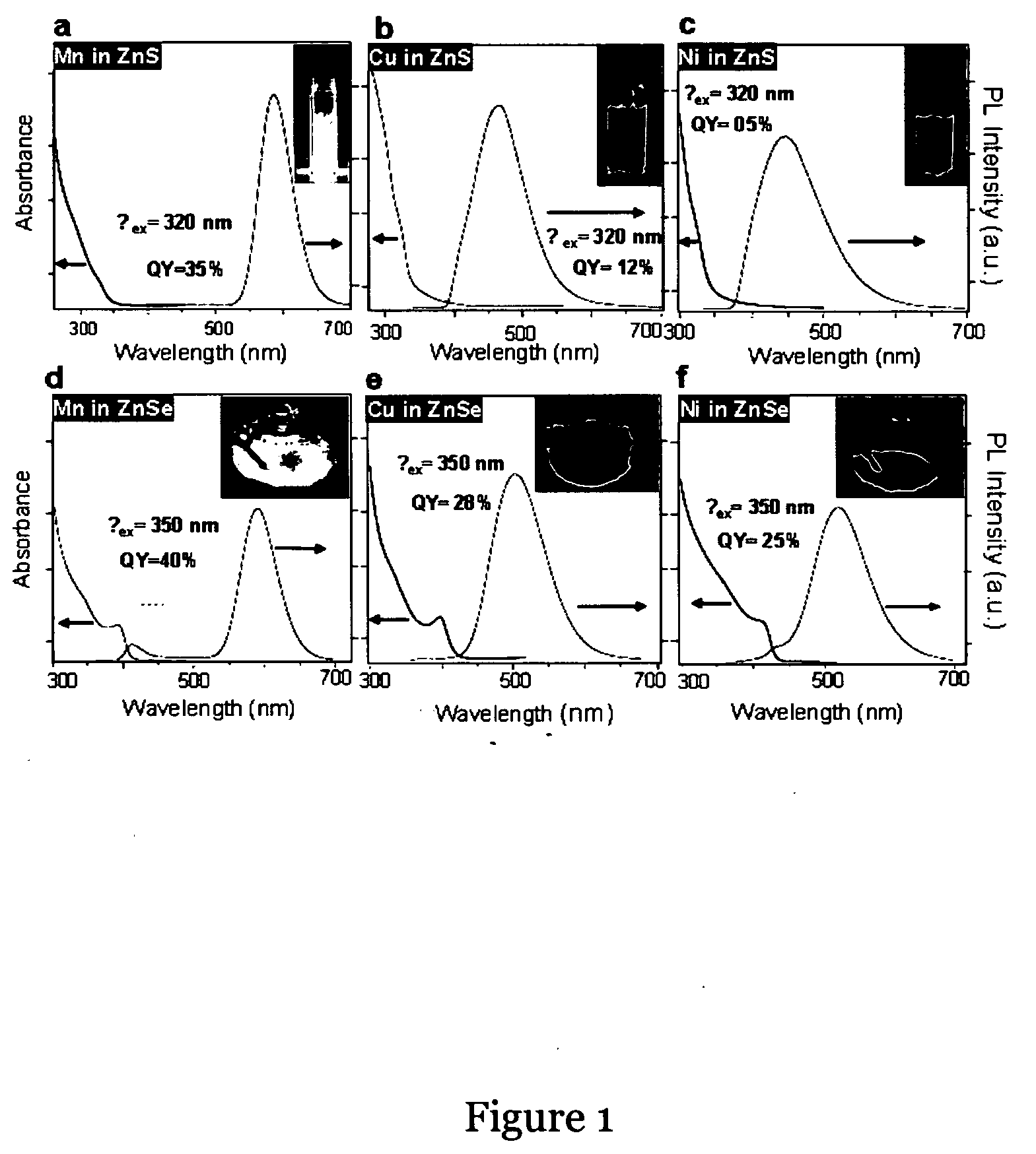
TABLE 1DopedColour ofMaterialsReported QYAchieved QYEmissionMn:ZnS18%36%Yellow-[J. Lumin., 60-61, 1994,orange275-280]Ni:ZnSNot reported5%GreenCu:ZnSNot reported 9%Blue-greenMn:ZnSe~50%30%Yellow-[Nano Lett., 2007, 7 (2),orange312-317]Ni:ZnSeNot reported25%GreenCu:ZnSe40% (unstable)40%...

Example

Example 3

Process for Estimating the Stability of the Transition Metal Ion Doped Semiconductor Nanocrystals in Air and Under UV Radiation in Solution and in the Precipitated Solid Form

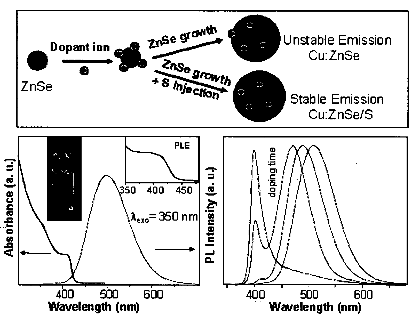
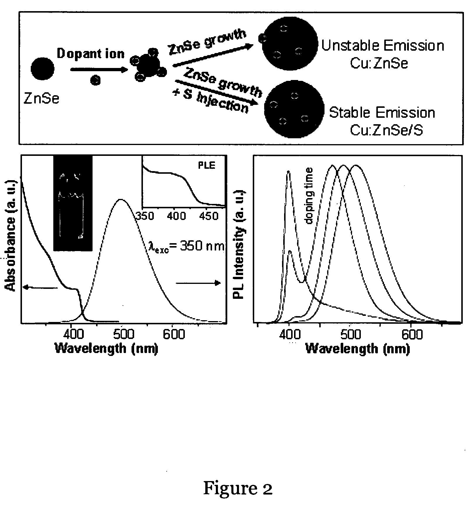
[0082]The stability was checked by keeping the powders open to air. For the UV irradiation experiments, the nanocrystal solution taken in chloroform and continuously irradiate with UV lamp. Doping emission is found stable in presence of calculated amount of Sulfur injection in the reaction mixture with enhanced intensity.

TABLE 2Temp. stabilityTemp StabilityEmission peakWaterin 1-Octadecenein waterpHTimeCompound(nm) and QYsolubility(at 300° C.)(100° C.)stabilitystabilityMn—ZnS~586 nm,YesYesYesYes stableAt least upMax QY = 40%from pH =to 6 MonthsStable Average5-930-36%Ni—ZnS~450-460—Yes——10 Days andQY = 05%then decreasesCu—ZnS~450-480YesYesYes—At least upQY = 09%to One MonthMn—ZnSe~580YesYesYespH-6-8At least upMax QY = 40%to 6 monthsStable Average25-30%Ni—ZnSe~490-530 nm—Yes——3 monthsQY = 25% under(Under ...


PUM


Abstract

The present invention deals with transition metal ions doped semiconductor nanocrystals that are free from heavy metals like cadmium and therefore environment friendly and useful for biological applications. The present invention also describes a process for the preparation of such transition metal ion doped semiconductor nanocrystals, where the reactions take place at a temperature less than 3000 C. The said doped nanocrystals are stable in air and under UV radiation in both solution and precipitated solid form.

Description

FIELD OF THE INVENTION[0001]The present invention relates to transition metal ion doped semiconductor nanocrystals and a process for the preparation thereof. The present invention more particularly relates to free-flowing, transition metal ions doped semiconductor nanocrystals comprising dopants and host nanocrystals.[0002]More preferably, the present invention relates to free-flowing, transition metal ions doped semiconductor nanocrystals comprising dopant ions selected from the group consisting of Mn, Ni, Cu and host nanocrystals selected from the group consisting of ZnS, ZnSe and ZnTe.[0003]The free-flowing transition metal ions doped semiconductor nanocrystals of the present invention have wide applications, including but not limiting to the preparation of light emitting diode, solar cell and bioimaging applications.BACKGROUND AND PRIOR ART OF THE INVENTION[0004]Fluorescing semiconductor nanomaterials e.g. CdSe are commonly known as quantum dots and are proven as stable bio-labe...

Claims


Application Information

Patent Timeline
IPC IPC(8): C09K11/88C09K11/08C09K11/56B82B1/00B82Y20/00B82Y40/00
CPCC09K11/565C09K11/883C09K11/574
Inventor PRADHAN, NARAYANJANA, NIKHIL RANJANDAS SARMA, DIPANKAR
Owner INDIAN ASSOC FOR THE CULTIVATION OF SCI
Why Eureka
Try Eureka