

Method to form solder deposits on substrates
a substrate and soldering technology, applied in the direction of cable/conductor manufacture, printed circuit manufacturing, semiconductor/solid-state device details, etc., can solve the problems of requiring various patterning steps, silicon chip and organic board structure has experienced an obvious explosive growth, and the flip chip device mounted on a low-cost organic circuit board has experienced a dramatic growth
- Summary
- Abstract
- Description
- Claims
- Application Information
AI Technical Summary
Benefits of technology
Problems solved by technology
Method used
Image

Examples
example 1
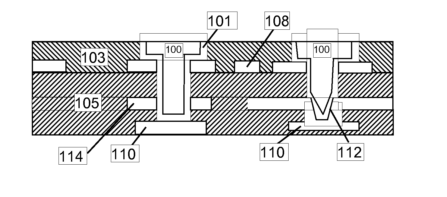
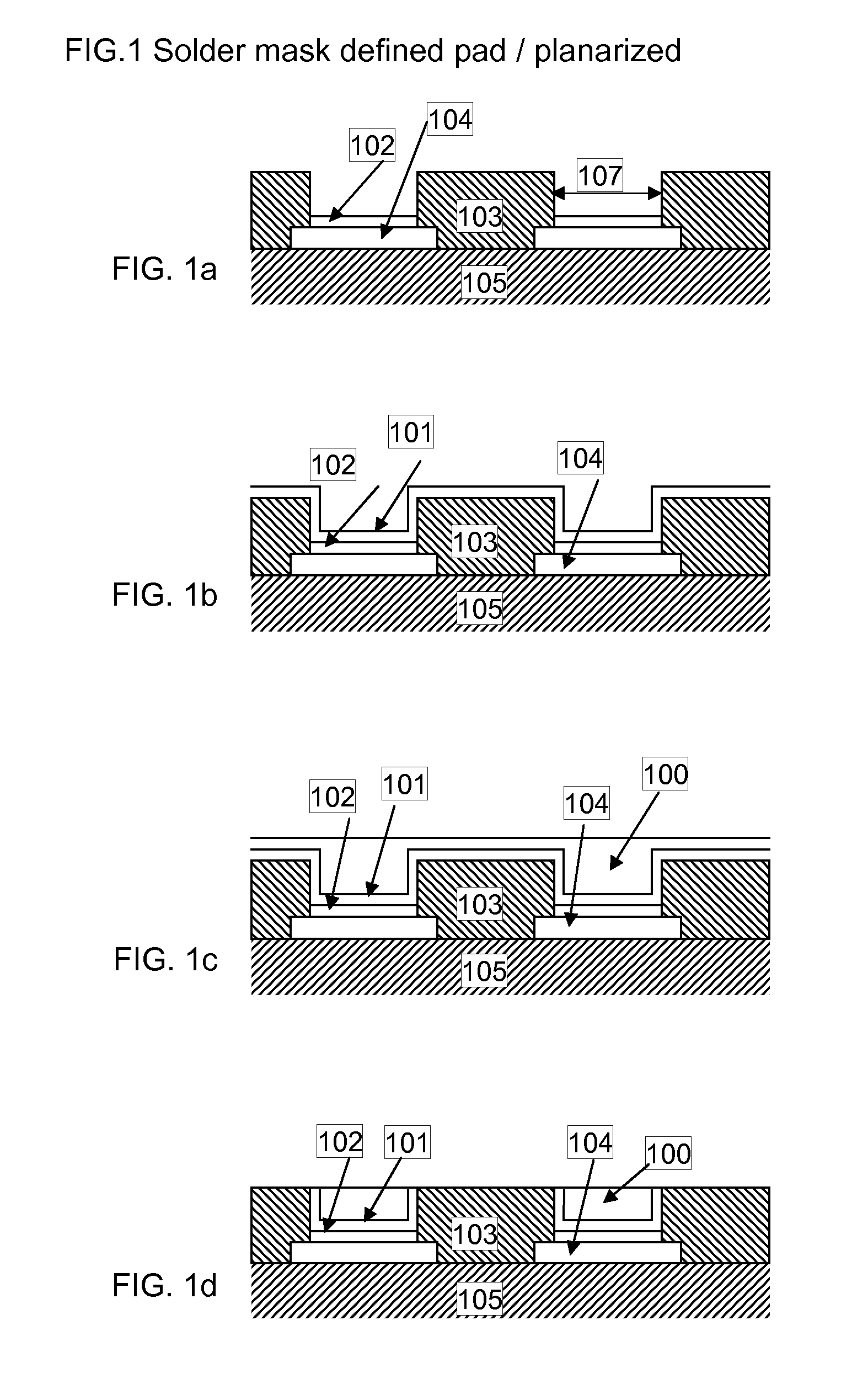
[0144]An IC substrate is used having a contact pad structure according to FIG. 1a. The SRO is 120 μm, the solder mask height is 25 μm.
[0145]The plating sequence is according to FIG. 1. First a conductive seed layer 101 of copper is formed on the entire substrate surface. For this the surface is first contacted with an acidic solution containing ionogenic palladium and then with a solution for chemical copper deposition.
[0146]Thereafter, a tin solder deposit 100 is plated on the conductive layer from a bath containing:
[0147]45 g / L Sn2+ as Sn(MSA)2, 60 mL / L MSA (70% solution), 2 g / L Hydroquinone, 7.0 g / L of Lugalvan BNO12 and 100 mg / L benzal acetone.
[0148]The pH of the bath is 0, the temperature 25° C. Plating is for 7 min. Pulse plating is used applying the following parameters:
[0149]Average current density of the forward current pulse: 2 A / dm2;
[0150]Duration of the forward current pulse: 20 ms;
[0151]Average current density of the reverse current pulse: 0 A / dm2 (no reverse pulse, onl...
example 2
[0156]Example 1 is repeated, now using a tin bath comprising 45 g / l Sn2+ as Sn(MSA)2, 60 ml / l MSA (70% solution), 0.5 g / l 2-amino-3-hydroxy-pyridin, 7.0 g / l of Lugalvan® BNO12 (a product of BASF SE) and a mixture of levelling agents consisting of 0.5 g / l methacrylic acid and 0.05 g / l 1-naphthaldehyde.
[0157]The tin solder deposit shows a very homogenous surface distribution and is whisker free. It is suited to be soldered to a chip or circuit.
PUM
| Property | Measurement | Unit |
|---|---|---|
| Electrical conductor | aaaaa | aaaaa |
| Area | aaaaa | aaaaa |
Abstract
Description
Claims
Application Information