Oxygen doping method to gallium nitride single crystal substrate

a gallium nitride and oxygen doping technology, applied in the direction of crystal growth process, crystal growth process, polycrystalline material growth, etc., can solve the problem that the device-carrying sapphire wafer cannot be divided by natural cleavage like silicon wafers, cannot make non-c-plane growing gan crystals at all, and induces plenty of dislocation, etc., to achieve high oxygen doping efficiency, high rate, and high indices of k- k0h

Inactive Publication Date: 2011-08-18
SUMITOMO ELECTRIC IND LTD
View PDF19 Cites 19 Cited by
  • Summary
  • Abstract
  • Description
  • Claims
  • Application Information

AI Technical Summary

Benefits of technology

[0063]{1-100} planes, in particular, are favorable planes for accepting oxygen with a high rate. {1-101} planes also sh

Problems solved by technology

Sapphire substrates cannot make non-C-plane growing GaN crystals at all.
Large lattice misfit between sapphire and gallium nitride induces plenty of dislocations in a gallium nitride crystal grown on a sapphire substrate.
When a plenty of device units have been fabricated upon a sapphire substrate wafer by wafer processes, the device-carrying sapphire wafer cannot be divided by natural cleavage like silicon wafers.
The mechanical dicing step raises the cost.
In the case of producing LDs (laser diodes) on sapphire substrates, the non-cleavage is a fatal drawback.
Another drawback results from the fact that sapphire is an insulator.
However, there is no mineral containing gallium nitride single crystals.
No attempt of making a wide, bulk GaN single crystal substrate artificially has succeeded until recently.
Since a GaN single crystal substrate was inaccessible, it was not possible to make GaInN type LEDs or LDs on a single crystal GaN substrate until recently.
The MOCVD is suffering from low yield and low growing speed.
The MOCVD is favorable for making thin GaN films but is unsuitable for producing a thick GaN crystal layer due to the material dissipation.
Another drawback is possib

Method used


Image

  • Oxygen doping method to gallium nitride single crystal substrate
  • Oxygen doping method to gallium nitride single crystal substrate
  • Oxygen doping method to gallium nitride single crystal substrate

Examples


embodiment 3

SUBSTRATE

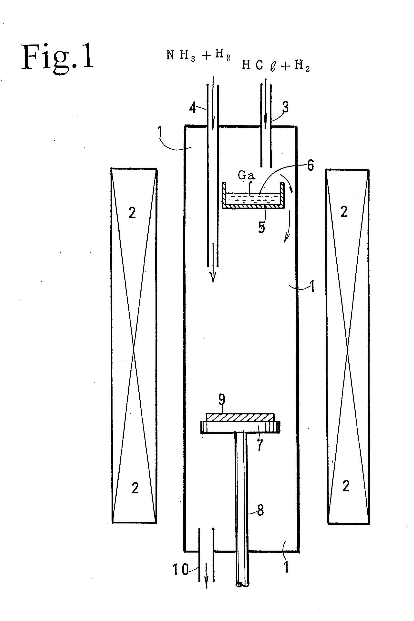
[0148]A 2-inch diameter (20-21) plane surface GaN seed single crystal which is produced by slicing a GaN single crystal ingot in parallel with (20-11) planes is prepared. The GaN single crystal ingot has been made by growing a thick C-plane surface GaN layer upon a sapphire C-plane undersubstrate in vapor phase and eliminating the sapphire undersubstrate.

[0149]The (20-21) plane surface of the GaN seed single crystal has been polished for removing a process-induced degradation layer. There is no process-induced degradation layer upon the top surface of the GaN seed single crystal.

[0150]A GaN crystal is grown upon the GaN seed crystal in vapor phase by the HVPE method. A carrier gas which contains about 2 ppm oxygen is used. The following is the conditions of the HYPE growth.[0151]Growth temperature: 1020°[0152]NH3 gas partial pressure: 0.2 atm (2×10⁴ Pa)[0153]HCl gas partial pressure: 1×10⁻² atm (1×10³ Pa)[0154]Growth time: 12 hours

[0155]GaN layer thickness: about 1000 μm

[01...

embodiment 4 (

[1-100] PLANE SURFACE WAFER)

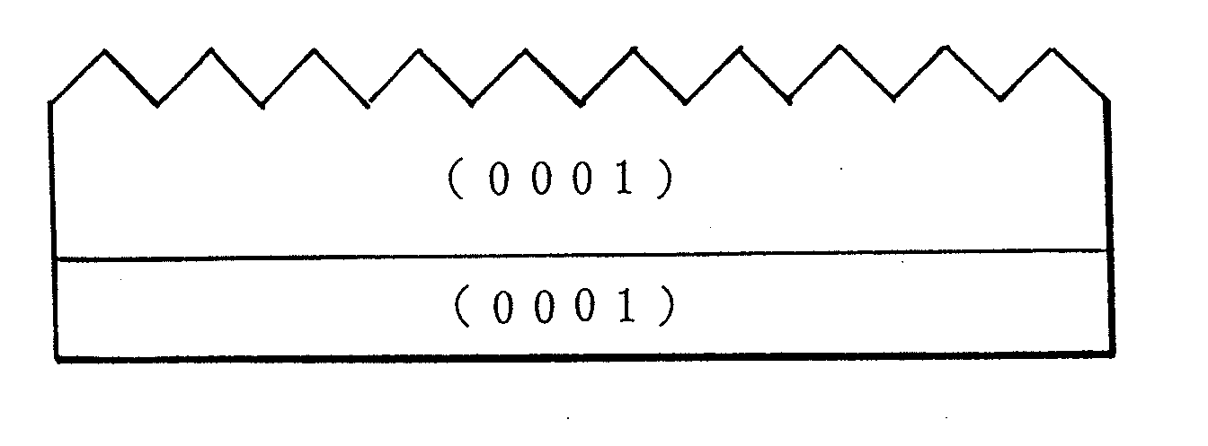
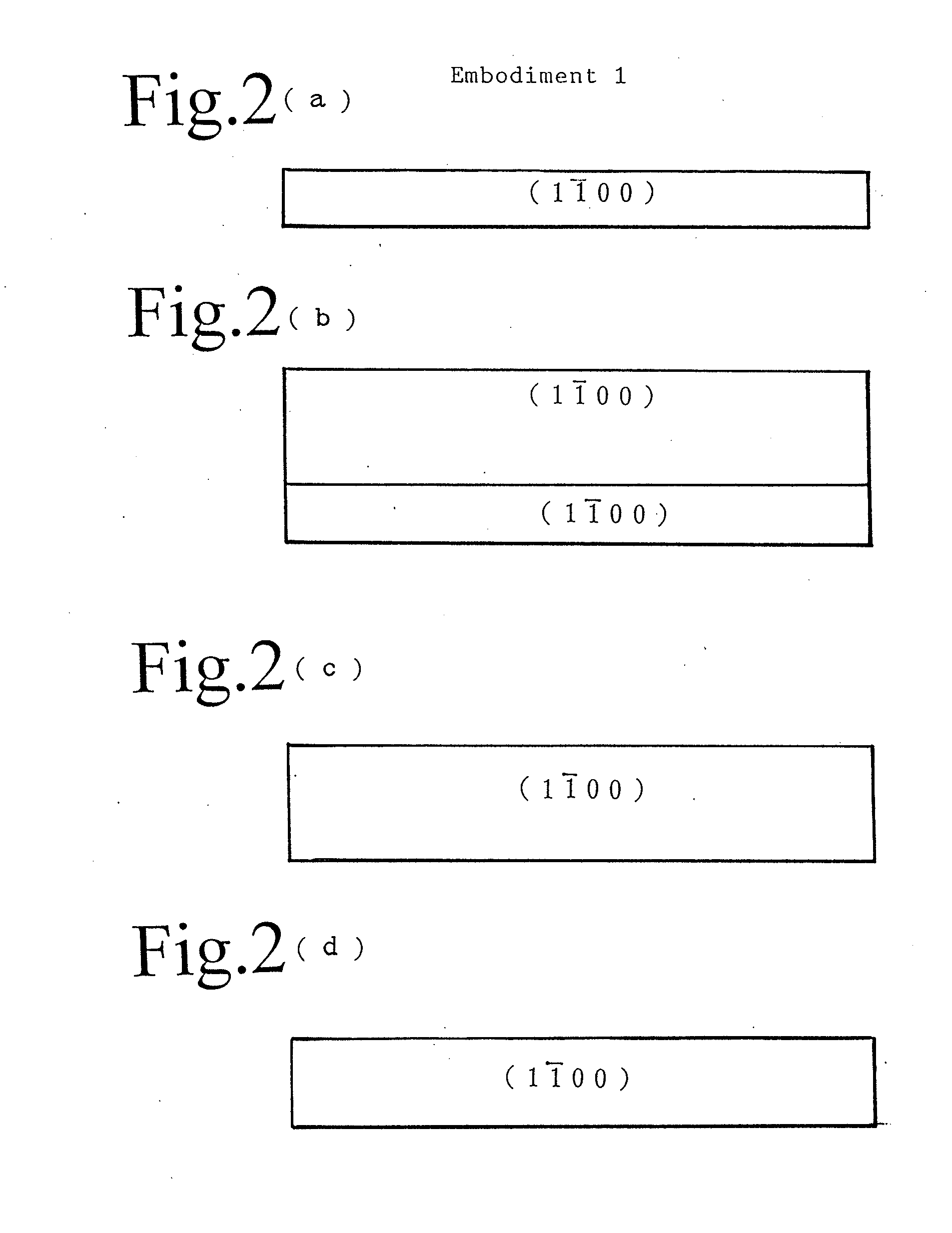
[0169]A 2-inch diameter M-plane ((1-100)) surface GaN seed single crystal which is produced by slicing a GaN single crystal ingot in parallel with (1-100) planes is prepared. The GaN single crystal ingot has been made by growing a thick C-plane surface GaN layer upon a sapphire C-plane undersubstrate in vapor phase and eliminating the sapphire undersubstrate. The cutting plane (1-100) is one of the parallel planes to the growing direction.

[0170]The surface of the M-plane GaN seed single crystal has been polished for removing a process-induced degradation layer. There is no process-induced degradation layer upon the top surface of the M-plane GaN seed single crystal.

[0171]A GaN crystal is grown upon the GaN seed crystal in vapor phase by the HVPE method. A carrier gas which contains water of about 1 ppm is used. The water is included as a source of oxygen. The following is the conditions of the HVPE growth.[0172]Growth temperature: 1020°[0173]NH3 gas parti...


PUM

PropertyMeasurementUnit
Lengthaaaaaaaaaa
Lengthaaaaaaaaaa
Dislocation densityaaaaaaaaaa

Abstract

Oxygen can be doped into a gallium nitride crystal by preparing a non-C-plane gallium nitride seed crystal, supplying material gases including gallium, nitrogen and oxygen to the non-C-plane gallium nitride seed crystal, growing a non-C-plane gallium nitride crystal on the non-C-plane gallium nitride seed crystal and allowing oxygen to infiltrating via a non-C-plane surface to the growing gallium nitride crystal. Oxygen-doped {20-21}, {1-101}, {1-100}, {11-20} or {20-22} surface n-type gallium nitride crystals are obtained.

Description

[0001]This application claims the priority of Japanese Patent Application No. 2001-113872 filed on Apr. 12, 2001 which is incorporated herein by reference. It is a continuation-in-part of application Ser. No. 12 / 652, 602 filed Jan. 5, 2010, which is a continuation of application Ser. No. 12 / 292,534 filed Nov. 20, 2008 and now issued as U.S. Pat. No. 7,667,298, which is a continuation of application Ser. No. 11 / 313,828 filed Dec. 22, 2005 and now issued as U.S. Pat. No. 7,470,970, which is a division of application Ser. No. 10 / 846,526, filed May 17, 2004 and is now issued as U.S. Pat. No. 7,012,318, which is a division of application Ser. No. 10 / 098,501, filed Mar. 18, 2002 and is now issued as U.S. Pat. No. 6,773,504, all of which are incorporated herein by reference in their entirety.BACKGROUND OF THE INVENTION[0002]1. Field of the Invention[0003]This invention relates to an oxygen doping method into a gallium nitride crystal and an oxygen-doped n-type gallium nitride single crysta...

Claims


Application Information

Patent Timeline
IPC IPC(8): H01L21/205
CPCC23C16/303H01L29/207C30B23/02C30B25/00C30B25/02C30B29/403C30B29/406C30B33/00H01L21/02389H01L21/02433H01L21/02458H01L21/02494H01L21/0254H01L21/02573H01L21/02609H01L21/0262H01L29/2003C30B23/00H01L21/02576H01L21/02645
Inventor MOTOKI, KENSAKUUENO, MASAKI
Owner SUMITOMO ELECTRIC IND LTD
Why Eureka
Try Eureka