Solar cell and method for fabricating the same

Inactive Publication Date: 2011-08-25
PANASONIC CORP
View PDF7 Cites 16 Cited by
  • Summary
  • Abstract
  • Description
  • Claims
  • Application Information

AI Technical Summary

Benefits of technology

[0038]The present invention allows the preparation of the solar cell directly on the graphite substrate with MOCVD by providing the amorphous carbon layer on the gr

Problems solved by technology

However, since the GaN film prepared on the graphite substrate by the pulse sputtering method is polycrystalline and has many defects, it is not suitable for a solar cell.
Furthermore, since the nitride semiconductor film prepared by a sputtering method is damaged severely due to discharged plasma during the film growth, it is well

Method used


Image

  • Solar cell and method for fabricating the same
  • Solar cell and method for fabricating the same
  • Solar cell and method for fabricating the same

Examples


embodiment 1

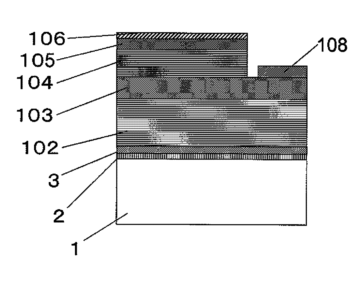
[0055]FIG. 1 shows a cross-sectional view of the solar cell according to the embodiment 1 of the present invention.

[0056]In FIG. 1, referential mark 1 indicates a graphite substrate. Referential mark 2 indicates an amorphous carbon layer which is caused to be amorphous by an oxygen-ashing treatment on the surface of the graphite substrate 1. The oxygen-ashing treatment includes a treatment by oxygen plasma. Referential mark 3 indicates an AlN layer formed on the amorphous carbon layer 2 with MOCVD.

[0057]A p-side electrode 107 which is a transparent electrode made of, for example, ITO (indium tin oxide) or a bilayer of nickel (Ni) and gold (Au) is formed on a p-type contact layer 106. An n-side electrode 108 made of a laminate film of titanium (Ti) and aluminum (Al) is formed on the upper surface of an n-type GaN layer 103.

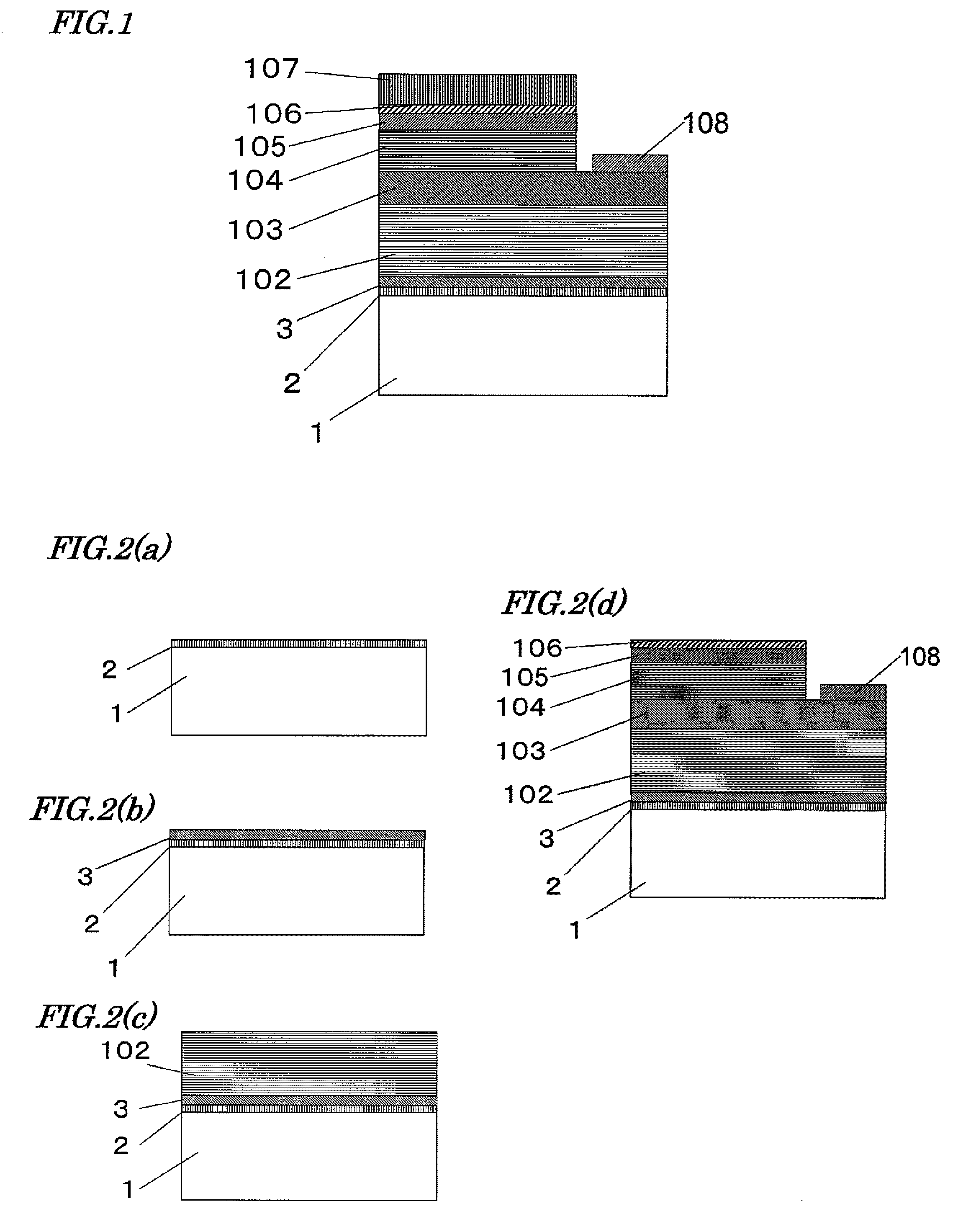
[0058]A fabrication method of the solar cell is described below with reference to the drawings.

[0059]FIG. 2(a) to FIG. 2(d) show cross-sectional views in the proce...

example 1

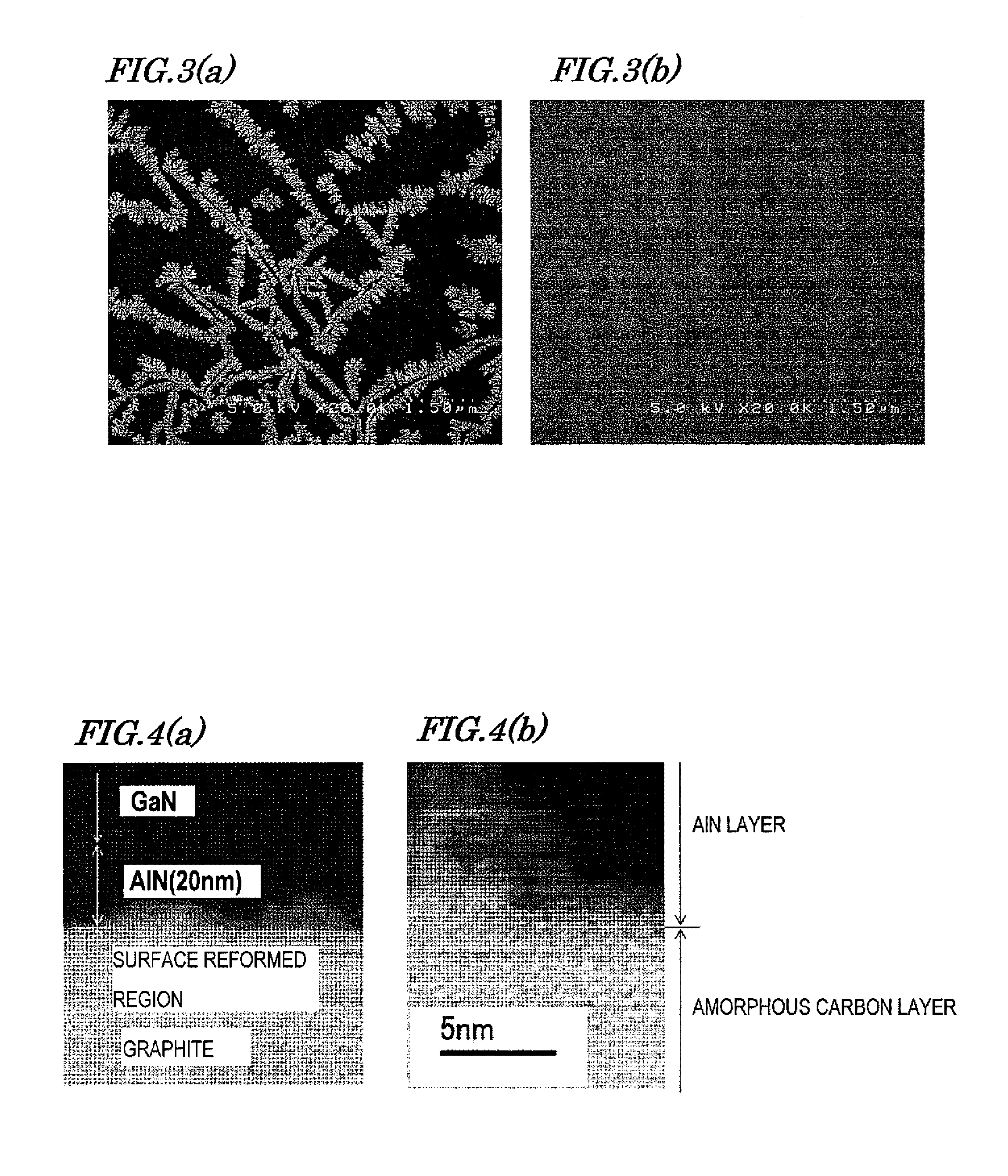
[0063]FIG. 3(a) shows the surface SEM observation image after AlN was deposited with MOCVD on the graphite substrate 1 where the surface treatment by the oxygen-ashing was not performed. FIG. 3(b) shows the surface SEM observation image after the AlN layer 3 with a thickness of 20 nanometers was formed with MOCVD on the graphite substrate provided with the amorphous carbon layer 2 with a thickness of 20 nanometers formed by the surface treatment of oxygen-ashing.

[0064]As is clear from FIG. 3(a), a dense AlN thin film was not formed on the graphite substrate 1 where the surface treatment of oxygen-ashing was not performed. Only a microcrystal such as a dendrite crystal was deposited. On the contrary, as is clear from FIG. 3(b), the dense AlN film was formed on the graphite substrate 1 provided with the amorphous carbon layer 2 on its surface.

[0065]FIG. 4(a) shows the cross-sectional TEM observation image of the substrate when the AlN layer 3 with a thickness of 20 nanometers formed w...

embodiment 2

[0082]FIG. 8 shows a cross-sectional view of the solar cell according to the embodiment 2 of the present invention. The difference from FIG. 1 lies in that the p-side electrode 109 is a zinc oxide (ZnO) film prepared by liquid phase synthesis.


PUM

PropertyMeasurementUnit
Nanoscale particle sizeaaaaaaaaaa
Energyaaaaaaaaaa

Abstract

A solar cell includes a graphite substrate, an amorphous carbon layer having a thickness of not less than 20 nm and not more than 60 nm formed on the graphite substrate, an AlN layer formed on the amorphous carbon layer, a n-type nitride semiconductor layer formed on the AlN layer; a light-absorption layer including a nitride semiconductor layer formed on the n-type nitride semiconductor layer; a p-type nitride semiconductor layer formed on the light-absorption layer; a p-side electrode electrically connected to the p-type nitride semiconductor layer; and an n-side electrode electrically connected to the n-type nitride semiconductor layer. The amorphous carbon layer is obtained by oxidizing the surface of the graphite substrate.

Description

[0001]This is a continuation of International Application No. PCT / JP2010 / 006224, with an international filing date of Oct. 20, 2010, which claims priority of Japanese Patent Application No. 2009-242006, filed on Oct. 21, 2009, the contents of which are hereby incorporated by reference.BACKGROUND OF THE INVENTION[0002]1. Field of the Invention[0003]The present invention relates to a solar cell composed of a nitride semiconductor.[0004]2. Description of the Related Art[0005]Recently, a semiconductor device composed of a nitride semiconductor such as gallium nitride (GaN) has been researched and developed actively. A semiconductor optical device made of nitride semiconductors such as aluminum nitride (AlN), gallium nitride (GaN), indium nitride (InN) or mixed crystal thereof absorbs light in a wide wavelength region from ultraviolet or blue to infrared by varying its film composition. The nitride semiconductor has a property of direct transition, and the light absorption coefficient th...

Claims


Application Information

Patent Timeline
IPC IPC(8): H01L31/06H01L31/0304H01L31/0352H01L31/0392H01L31/0735H01L31/18
CPCC23C16/303C30B25/183C30B25/186C30B29/403H01L21/02376H01L21/0243Y02E10/544H01L21/0254H01L21/0262H01L21/02658H01L31/0392H01L31/0693H01L31/1852H01L21/02458Y02P70/50
Inventor NAGAO, NOBUAKIHAMADA, TAKAHIROITOH, AKIHIRO
Owner PANASONIC CORP
Why Eureka
Try Eureka