Method for producing a layer system on a substrate and layer system

a technology of layer system and substrate, applied in the direction of ion implantation coating, chemical vapor deposition coating, coating, etc., can solve the problems of unfavorable transmission and reception loss, color impression is very sensitively dependent, and complicated process configuration disadvantages, etc., to achieve high sheet resistance

Inactive Publication Date: 2011-09-15
LEYBOLD OPTICS
View PDF17 Cites 21 Cited by
  • Summary
  • Abstract
  • Description
  • Claims
  • Application Information

AI Technical Summary

Benefits of technology

[0037]Owing to the high sheet resistance, the housing is transmissive for radiofrequency radiation between 400 MHz and 5 GHz, but it nevertheless has a metallic or colored appearance. The housing is furthermore lightweight if the substrate material is plastic, for example polycarbonate.

Problems solved by technology

Electrically conductive metal layers would at least partially reflect the radio waves in the conventionally used frequency range of about 400 MHz to about 5 GHz, and thus lead to undesired transmission and reception losses.
A disadvantage with these layer systems is that the resulting color impression is very sensitively dependent on layer thickness variations.
The document JP 05 065 650 A discloses the production of a dielectric layer with embedded metal particles, although it has the disadvantage of complicated process configuration.
For example, high yield losses of up to 60% due to lacquering defects are often reported.
Furthermore, a plurality of lacquer layers are usually necessary (colored lacquer, clear hard lacquer), which entails extra costs.

Method used


Image

  • Method for producing a layer system on a substrate and layer system
  • Method for producing a layer system on a substrate and layer system
  • Method for producing a layer system on a substrate and layer system

Examples


Embodiment Construction

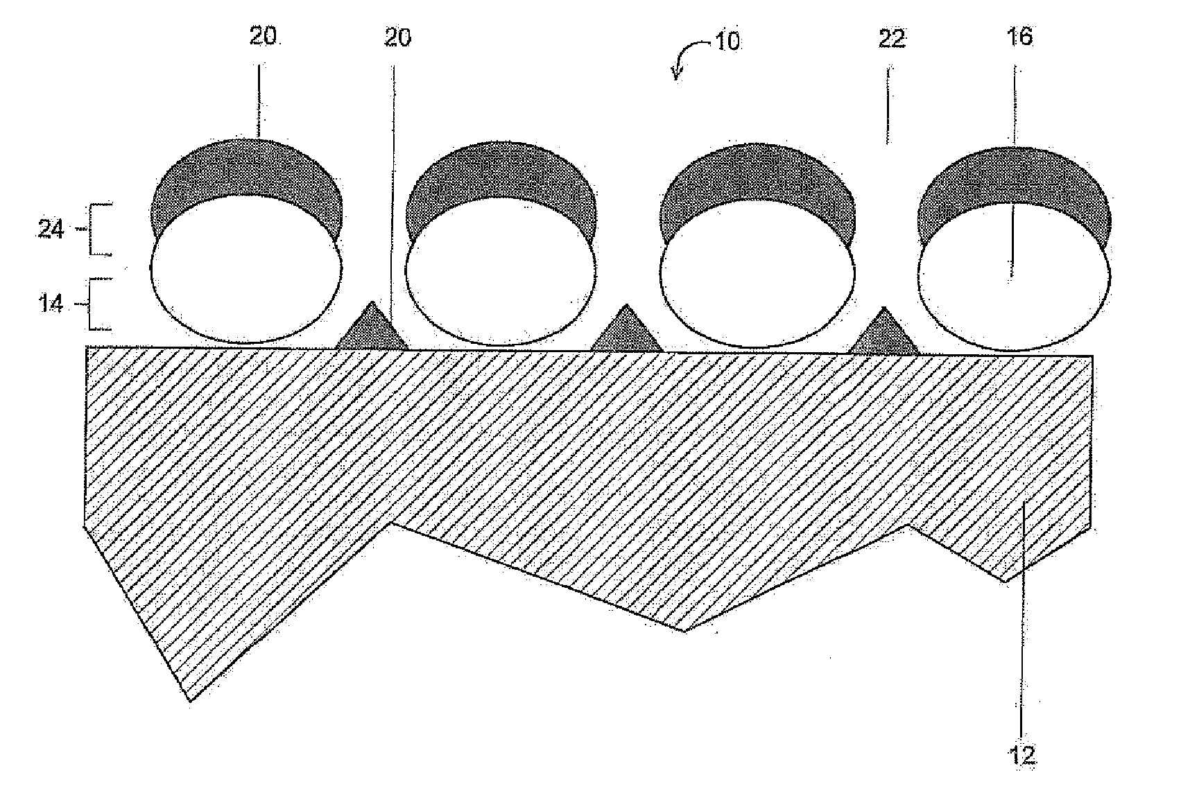
[0042]FIG. 1 schematically represents a layer system which is applied on a dielectric substrate 12. The substrate 12 is preferably produced from a dielectric material, in particular plastic. The substrate 12 particularly preferably consists of polycarbonate. The substrate 12 may be a housing body, for example for a mobile telephone, a laptop or another electrical or electronic device, or part of a housing. Of course, the housing may also be provided for a static device.

[0043]The layer 14 applied directly on the substrate 12 comprises islands 16, which contain a metal element or a metal alloy. The islands 16 form a discontinuous metal layer on the substrate 12. Valleys 22 are formed between the islands 16. The metal layer has a sheet resistance >10 Mohm.

[0044]A further layer 24 is applied, preferably also by means of a vacuum process, onto the metal layer 14 described above. The further layer 24 likewise comprises islands 20, so that a discontinuous layer is also formed by the furthe...


PUM

PropertyMeasurementUnit
reflectanceaaaaaaaaaa
thicknessaaaaaaaaaa
thicknessaaaaaaaaaa

Abstract

In the method for producing a layer system on a dielectric substrate in which a metal layer is applied onto the substrate by a coating step (110) and a further layer with a predetermined layer thickness is subsequently applied by a further coating step (140), the metal layer having a sheet resistance >10 Mohm and an average reflectance >50%, the further layer would have a sheet resistance <1 Mohm if it had been applied onto the substrate with the same layer thickness by the further coating step (140), and the layer system consisting of the metal layer and the further layer has a sheet resistance >10 Mohm, where the invention furthermore relates to a layer system on a dielectric substrate in which a metal layer is applied onto the substrate by a coating step (110) and a further layer with a predetermined layer thickness is subsequently applied by a further coating step (140), the metal layer having a sheet resistance >10 Mohm and an average reflectance >50%, where the further layer, if it had been applied onto the substrate with the same layer thickness by the further coating step (140), would have a sheet resistance <1 Mohm, and the layer system consisting of the metal layer and the further layer has a sheet resistance >10 Mohm, the invention further providing a housing including a layer system.

Description

TECHNICAL FIELD[0001]The present invention relates to a method for producing a layer system on a substrate, and to a layer system on a substrate, respectively corresponding to the precharacterizing clauses of the independent patent claims. The invention furthermore relates to a housing, comprising such a layer system, for an electrical device.BACKGROUND[0002]The metallization of dielectric substrates, for example by means of vacuum metallization, has already been known for some time. For example, thermal evaporation or sputtering may be used as vacuum metallization methods.[0003]At least since the U.S. Pat. No. 4,431,711, it has furthermore been known that metals, for example indium (In) or tin (Sn), can initially grow by island growth during vacuum metallization. Thin layers of these metals then consist of islands which are not in electrical contact with one another. These layers already have optical properties of the metal—for example metallic sheen—but are not conductive and can ...

Claims


Application Information

Patent Timeline
Patent Type & Authority Applications(United States)
IPC IPC(8): H05K5/00H05K1/00H05K1/09B05D1/36C23C16/44C23C16/50B05D5/00B05D5/06C23C14/34C23C14/06
CPCC23C14/0015C23C14/025C23C16/006C23C14/0641C23C14/04
Inventor PISTNER, JURGENSCHMAUDER, TORSTENKUPER, STEPHAN
Owner LEYBOLD OPTICS
Why Eureka
Try Eureka