Semiconductor device and method for manufacturing the same

a semiconductor and semiconductor technology, applied in the direction of semiconductor devices, electrical equipment, transistors, etc., can solve the problems of increasing causing short-channel effects, and easy to cause short-channel effects, so as to reduce the amount of heat generation or power consumption of the transistor in the upper layer which is electrically connected to the wiring or the electrode in the lower layer. , the effect of reducing the amount of heat generation or power consumption of the transistor in the upper

Inactive Publication Date: 2011-09-15
SEMICON ENERGY LAB CO LTD
View PDF103 Cites 17 Cited by
  • Summary
  • Abstract
  • Description
  • Claims
  • Application Information

AI Technical Summary

Benefits of technology

[0044]According to an embodiment of the disclosed invention, a channel formation region of a transistor is provided in an extremely flat region, whereby a problem such as a short-channel effect can be prevented even when the transistor is miniaturized and thus a transistor having favorable characteristics can be provided.
[0045]Moreover, according to an embodiment of the disclosed invention, part of a top surface of a wiring or an electrode in a lower layer is formed in a higher position than part of a surface of an insulating layer, whereby a reduction in the area of a portion where the wiring or the electrode in the lower layer is in contact with an electrode of a transistor in an upper layer can be prevented and thus the contact resistance between the wiring or t

Problems solved by technology

In the case where a transistor is miniaturized, a problem of a short-channel effect is caused.
In particular, since threshold voltage of a transistor including an oxide semiconductor cannot be controlled by impurity doping unlike a transistor including silicon, the short-channel effect tends to be caused easil

Method used


Image

  • Semiconductor device and method for manufacturing the same
  • Semiconductor device and method for manufacturing the same
  • Semiconductor device and method for manufacturing the same

Examples


embodiment 1

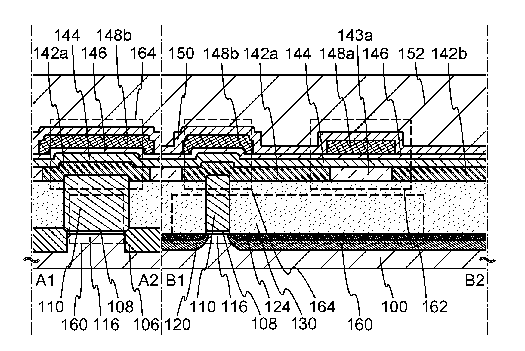
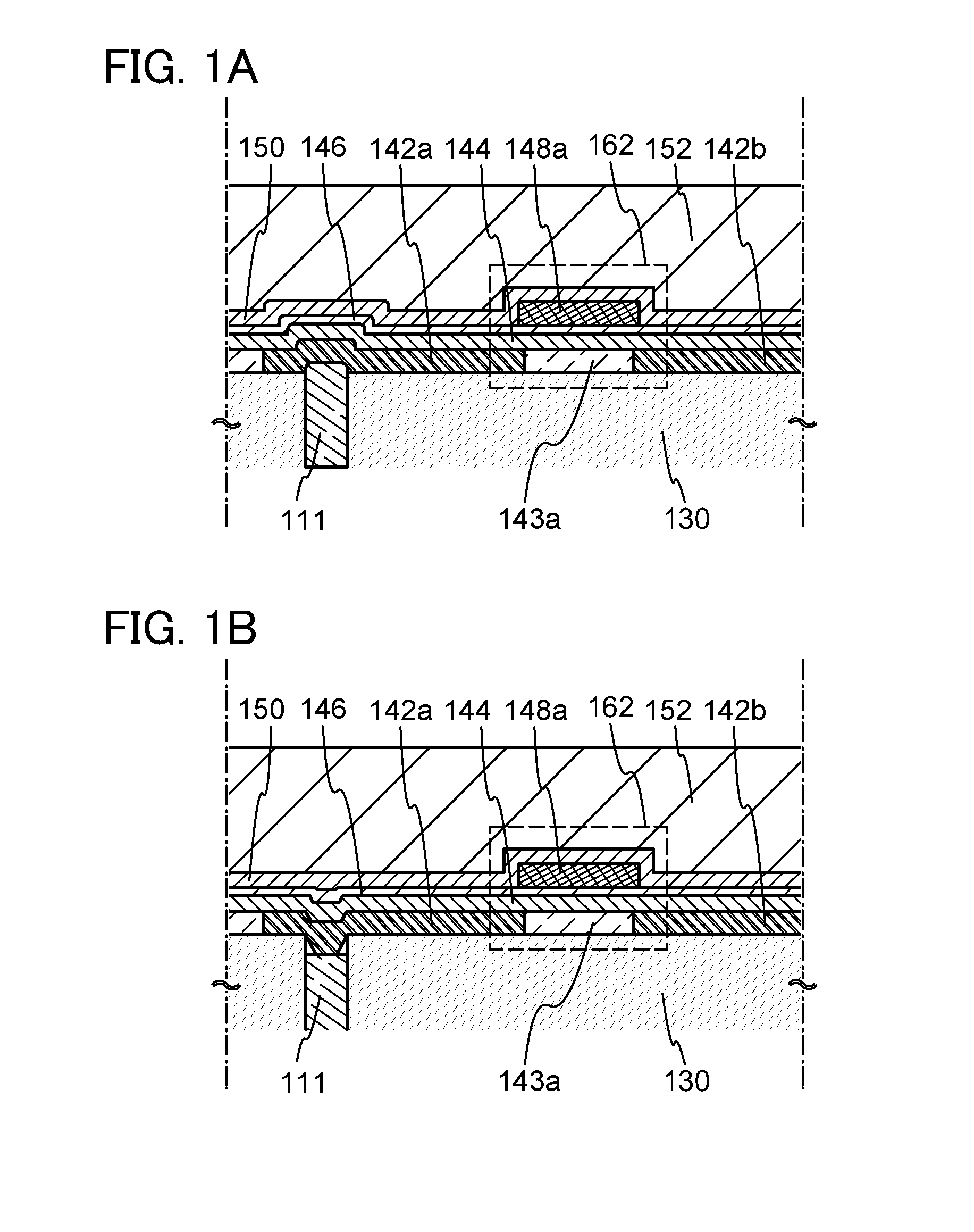
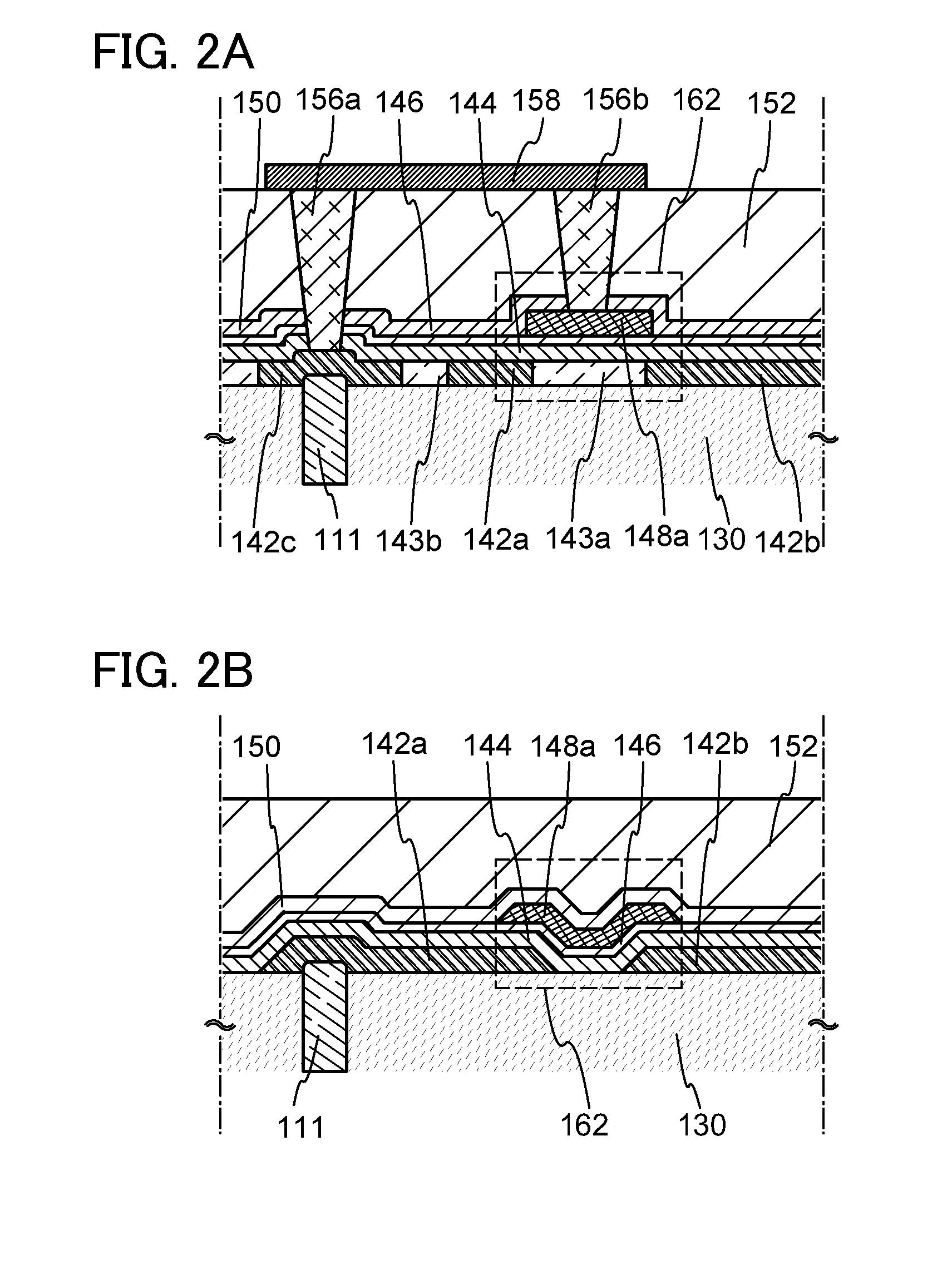
[0065]In this embodiment, a structure and a manufacturing method of a semiconductor device according to an embodiment of the disclosed invention will be described with reference to FIGS. 1A and 1B, FIGS. 2A and 2B, FIGS. 3A to 3E, and FIGS. 4A to 4C.

[0066]FIG. 1A illustrates an example of a structure of a semiconductor device including a transistor 162 which is formed over an insulating layer 130 where a wiring 111 is embedded and which is electrically connected to the wiring 111 via a source electrode 142a.

[0067]The transistor 162 illustrated in FIG. 1A includes an insulating layer 143a formed over the insulating layer 130 where the wiring 111 is embedded; the source electrode 142a and a drain electrode 142b embedded in an insulating layer including the insulating layer 143a; an oxide semiconductor layer 144 partly in contact with a top surface of the insulating layer 143a, a top surface of the source electrode 142a, and a top surface of the drain electrode 142b; a gate insulating...

embodiment 2

[0153]In this embodiment, a structure and a manufacturing method of a semiconductor device according to another embodiment of the disclosed invention will be described with reference to FIGS. 5A to 5C, FIGS. 6A to 6C, FIGS. 7A to 7D, and FIGS. 8A to 8C.

[0154]FIGS. 5A to 5C illustrate an example of a structure of a semiconductor device. FIGS. 5A to 5C illustrate a cross-sectional view, a plan view, and a circuit configuration of the semiconductor device, respectively. Note that operation of the semiconductor device will be described in detail in the following embodiment; in this embodiment, the structure of the semiconductor device will be mainly described. Note that the semiconductor device illustrated in FIGS. 5A to 5C is an example of a semiconductor device having a predetermined function and does not exhaustively represent the semiconductor device of the disclosed invention. The semiconductor device according to the disclosed invention can have another function by changing connec...

embodiment 3

[0200]In this embodiment, an application example of a semiconductor device according to an embodiment of the disclosed invention will be described with reference to FIGS. 9A to 9C. Here, an example of a memory device will be described. Note that in circuit diagrams, “OS” may be written beside a transistor in order to indicate that the transistor includes an oxide semiconductor.

[0201]In the semiconductor device illustrated in FIG. 9A, which can be used as a memory device, a first wiring (1st Line) is electrically connected to a source electrode of a transistor 1000, and a second wiring (2nd Line) is electrically connected to a drain electrode of the transistor 1000. A gate electrode of the transistor 1000 and one of a source electrode and a drain electrode of a transistor 1010 are electrically connected to one electrode of a capacitor 1020. A third wiring (3rd Line) and the other of the source electrode and the drain electrode of the transistor 1010 are electrically connected to each...


PUM


Abstract

A semiconductor device includes a wiring embedded in an insulating layer, an oxide semiconductor layer over the insulating layer, a source electrode and a drain electrode electrically connected to the oxide semiconductor layer, a gate electrode provided to overlap with the oxide semiconductor layer, and a gate insulating layer provided between the oxide semiconductor layer and the gate electrode. The insulating layer is formed so that part of a top surface of the wiring is exposed. The part of the top surface of the wiring is positioned higher than part of a surface of the insulating layer. The wiring in a region exposed from the insulating layer is electrically connected to the source electrode or the drain electrode. The root-mean-square roughness of a region which is part of the surface of the insulating layer and in contact with the oxide semiconductor layer is 1 nm or less.

Description

TECHNICAL FIELD[0001]The technical field of the invention relates to a semiconductor device and a method for manufacturing the semiconductor device. Here, semiconductor devices refer to general elements and devices which function by utilizing semiconductor characteristics.BACKGROUND ART[0002]There are a wide variety of metal oxides and such metal oxides are used for various applications. Indium oxide is a well-known material and has been used as a material of transparent electrodes needed in liquid crystal display devices or the like.[0003]Some metal oxides have semiconductor characteristics. Examples of such metal oxides having semiconductor characteristics are tungsten oxide, tin oxide, indium oxide, zinc oxide, and the like. A thin film transistor in which a channel formation region is formed using such a metal oxide is already known (e.g., see Patent Documents 1 to 4, Non-Patent Document 1, and the like).[0004]As metal oxides, not only single-component oxides but also multi-comp...

Claims


Application Information

Patent Timeline
IPC IPC(8): H01L29/786H01L21/336
CPCH01L27/124H01L27/1225
Inventor FUJII, TERUYUKIIMAHAYASHI, RYOTA
Owner SEMICON ENERGY LAB CO LTD
Why Eureka
Try Eureka