Method of manufacturing transparent conductive film

a technology of transparent conductive film and manufacturing method, which is applied in the direction of oxide conductors, non-metal conductors, plasma techniques, etc., can solve the problems of decreased film quality, increased resistance, and increased resistance, so as to achieve higher light confinement effect and value of ra

Inactive Publication Date: 2011-10-06
FUJIFILM CORP
View PDF9 Cites 17 Cited by
  • Summary
  • Abstract
  • Description
  • Claims
  • Application Information

AI Technical Summary

Benefits of technology

[0129]The substrate Z was peeled off, and the surface of the zinc oxide transparent conductive film was observed by AFM (atomic force microscope). The light confinement effect of the zinc oxide transparent conductive film was evaluated by measuring the center line average roughness Ra (measurement length=10 micrometers). The higher the value of Ra, the higher the light confinement effect it was considered to have, as it was judged that a textured structure was efficiently generated. The evaluations were as follows.
[0134]For resistivity and light confinement effect, ⊚ was given 3 points, ◯ was given 2 points, Δ was given 1 point, and x was given 0 points. These were totaled, and the overall evaluation of the film was scored as follows:

Problems solved by technology

Incidentally, streamers (localized weak current) generated by the discharge unit have been cited as a cause of decreased quality of the formed film in atmospheric pressure plasma-enhanced CVD by dielectric barrier discharge of prior art, including the film formation method described in JP 2004-235004 A.
When streamers are generated by the discharge unit during formation of a transparent conductive film, disorder of crystal growth of the film is caused, and resistivity ends up becoming worse.
That is, streamers tend to invite generation of particles.
When particles are mixed into the film, growth of crystals from the substrate surface in the perpendicular direction is hindered, and as a result, crystal growth of the film ends up becoming inadequate.
However, although it is not thought to be difficult to produce this transparent conductive film having a textured structure when film formation is performed at low pressure, it is difficult to obtain such a textured structure if the transparent conductive film is formed by treating a large-area film roll, etc., at atmospheric pressure.

Method used


Image

  • Method of manufacturing transparent conductive film
  • Method of manufacturing transparent conductive film

Examples


example 1

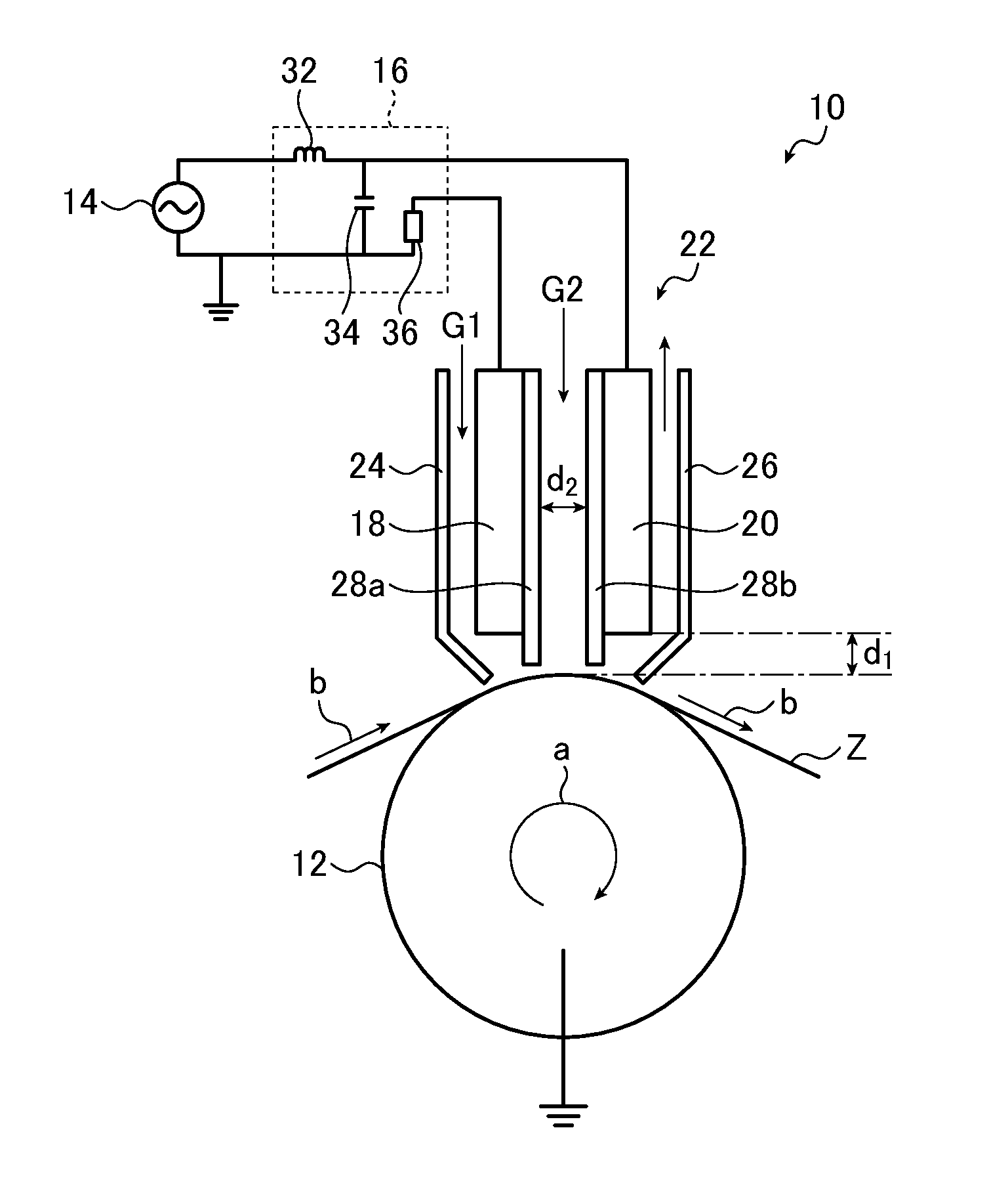
[0102]The film formation apparatus 10 shown in FIG. 1, which performs film formation by atmospheric pressure plasma-enhanced CVD by dielectric barrier discharge (DBD), was used to form a zinc oxide transparent conductive film with a thickness of 150 nm on the surface of a substrate Z.

[0103]As the substrate Z, a polyimide film with a thickness of 0.1 mm was used.

[0104]As the oxygen atom supply gas G1, 99.999% oxygen was used. The oxygen atom supply gas G1 was made to flow at a rate of 10 liters per minute, and by passing it through a UV radiation device, ozone was generated and then supplied between the flow path member 24 and the insulating plate 28a. Note that the UV radiation device irradiated ultraviolet light of 185 nm and 254 nm using the ozone lamp NIQ120 / 44U made by Heraeus. The radiation intensity was 0.06 W / cm2.

[0105]Diethyl zinc (Zn(C2H5)2) was supplied (4 g / hour) as a liquid to a vaporizer and was vaporized while heating to 100° C., and this was used as the gaseous raw ma...

example 2

[0111]A zinc oxide transparent conductive film with a thickness of 150 nm was formed on the surface of a substrate Z in the same way as in example 1, except that trimethyl aluminum (TMAl) was used instead of Al(DIBM)3 as the gaseous raw materials (film forming material).

[0112]Note that TMAl was supplied (0.1 g / hour) to the vaporizer as a liquid at 100° C., and it was vaporized while being sprayed, to form the gaseous raw material. Using nitrogen gas as a carrier gas (flow rate 2 L / minute), the vaporized TMAl was supplied between the insulating plates 28a and 28b, and it was mixed with diethyl zinc to form the film forming gas G2.

[0113]The film formation rate was 1200 nm / minute.

example 3

[0114]A zinc oxide transparent conductive film with a thickness of 150 nm was formed on the surface of a substrate Z in the same way as in example 1, except that Zn(OD)2 was used instead of diethyl zinc as the gaseous raw material (film forming raw material).

[0115]Note that a toluene solution of Zn(OD)2 in a concentration of 0.05 mol / L was used to supply Zn(OD)2. This solution was introduced into the vaporizer at a flow rate of 0.1 g / hour, and by heating it to 200° C., the Zn(OD)2 was vaporized, and gaseous raw material was obtained. Using nitrogen gas as a carrier gas (flow rate 2 L / minute), this gaseous raw material was supplied between the insulating plates 28a and 28b, so as to hold the pressure inside the vaporizer at 0.01 MPa above atmospheric pressure, and it was mixed with Al(DIBM)3 to form the film forming gas G2.

[0116]The film formation rate was 1100 nm / minute.


PUM

PropertyMeasurementUnit
temperatureaaaaaaaaaa
distanceaaaaaaaaaa
distanceaaaaaaaaaa

Abstract

An atmospheric-pressure plasma-enhanced MOCVD (metal organic chemical vapor deposition) uses a power circuit for supplying power for plasma generation, including a pulse control circuit provided inside in order to form a transparent conductive film on the surface of the substrate, the transparent conductive film having a low resistivity, excellent optical characteristics and a good texture formed on the surface using dielectric barrier discharge.

Description

BACKGROUND OF THE INVENTION[0001]The present invention relates to a method of manufacturing a transparent conductive film that enables stable formation of a transparent conductive film having low resistance and superior optical characteristics.[0002]For example, as the upper electrode of a solar cell (electrode on the side nearest the light impinging surface), transparent conductive films such as zinc oxide, indium zinc oxide (IZO), indium tin oxide (ITO) and tin oxide are used. In particular, zinc oxide has the advantages that the raw material is plentiful and it has safety excellent enough to be used in pigments.[0003]Sputtering has been widely used as the method of forming such transparent conductive films. Further, as a simple method to replace sputtering, research and development are being conducted in various places on MOCVD (metal organic chemical vapor deposition) using atmospheric pressure plasma.[0004]For example, JP 2004-235004 A describes a film formation method for IZO ...

Claims


Application Information

Patent Timeline
Patent Type & Authority Applications(United States)
IPC IPC(8): B05D5/12C08J7/18
CPCC23C16/407C23C16/452C23C16/515Y02E10/50H01B1/08H01L31/1884C23C16/545
Inventor TAKANO, NOBUHIKO
Owner FUJIFILM CORP
Why Eureka
Try Eureka