Device for detecting highly energetic photons

a high-energy photon and detector technology, applied in the field of positron emission tomography, can solve the problems of limited energy resolution, reduced the ability to remove scattered events, and error in the projection of the line of response, so as to achieve the effect of considerably worse spatial resolution

Active Publication Date: 2011-10-20
INST DE FISICA D ALTES ENERTIES (IFAE)
View PDF5 Cites 22 Cited by
  • Summary
  • Abstract
  • Description
  • Claims
  • Application Information

AI Technical Summary

Benefits of technology

[0026]It is a further object of the present invention to provide a device for detecting highly energetic photons with a high spatial resolution and a high detection efficiency. High spatial resolution provides exact location (x,y,z) of the impact point of the gamma photon; high detection efficiency helps in the reduction of radiation doses.
[0027]Another object of the present invention is to provide a device for detecting highly energetic photons with improved energy resolution to eliminate a large fraction of the scattered events and increase the Signal-to-Noise ratio (SNR). This leads to a high contrast image.
[0029]Instead of using a scintillating crystal (with its mentioned inconveniences), the invention provides a pixelated solid state detector for detecting highly energetic photons. A typical pixel size may be 1 mm×1 mm, but it is possible to make pixelated solid state detectors with pixel sizes of e.g. 10 μm×10 μm. The invention thus offers a tremendous potential of spatial precision. This precision can never be reached using scintillating crystals. A device may thus be tailored to specific needs in different applications. It is even possible to vary the pixel size within a single solid-state detector. Also, there are no dead areas between the pixels of the detectors. Even an event occurring between two pixels can still be detected by two pixels together.
[0030]Additionally, because of its modular and simple built-up, a plurality of devices can easily be combined to appropriate size in three dimensions.
[0033]The typical thickness of the solid-state detectors used in the devices may be 2 mm (but other thicknesses are of course possible). It is possible to combine a plurality of these devices to an appropriate thickness without encountering problems related to e.g. time collection of thick conventional solid state detectors.
[0034]Moreover, the invention provides a detector which can be used in strong magnetic fields. A detector based on the invention can thus be combined with e.g. an MRI scanner into a single scanner, which allows a PET scan and an MRI scan to be performed simultaneously.

Problems solved by technology

This limited energy resolution will reduce the ability to remove scattered events, which are one type of noise in the reconstructed image.
The typical length (in radial direction, when used in a PET scanner) of the LSO crystal is about 10 mm and this implies that the detector's intrinsic uncertainty of the impact point in the radial direction is around 3 mm, which will lead to an error in the projection of the Line of Response.
This loss of information gives rise to a parallax effect, which can lead to an error in the projection of the LOR.
This error naturally deteriorates the quality of the reconstructed image.
Another drawback is the shape of the crystals of the detector, which is rectangular parallelepiped and when forming a cylindrical shape from such components (for example, for a PET scanner), it is inevitable to have cracks at the contact points of the crystals.
The detectors based on scintillating crystals suffer from various disadvantages: In PET scanners, cracks are inherently present at the contact points of adjacent parallelepiped crystals.
It is not possible to see anything smaller than 4-5 mm in case of PET scanning.
The spatial resolution will even be considerably worse since the detectors do not work with 100% efficiency.
Another problem with scintillating crystals is that the Detection Quantum Efficiency (DQE) of scintillating crystals is rather poor.
However, adding more material would not necessarily improve the quality of the signal, since a part of the light produced in the crystals at a location that is relatively far away from the photomultiplier would be attenuated before reaching the PMT.
Hence, the energy resolution gets worse at the expense of detecting more gamma photons.
One of the problems of using solid-state detectors in a PET scanner is that thick detectors are needed to achieve high gamma ray absorption.
Firstly, the cost of such large CdTe detectors of good quality is very high.
Secondly, the time collection of the signal will be very long and hence it will not be possible to use it in PET as trigger.
Thirdly, with such a thick detector (10 mm), the energy spectroscopy deteriorates significantly due to trapping and the lifetime of the electron-hole.
Since the detectors used in this system are not pixelated, the accuracy that may be achieved is inherently limited.
The accuracy is thus limited to these dimensions.
Furthermore, in practice it will be very complicated and costly to use detectors of these dimensions, so that bigger detectors will be needed.
Also, between all of the detectors, gaps are present.
These gaps, which represent dead areas in which no events can be detected, and the way the arrays of detectors are packaged and arranged lead to limited detection efficiency.
The wiring used to connect an individual detector to the pre-amplifier leads to parasitic capacitance, inductance and resistance and therefore increases the over all noise to signal ratio.

Method used


Image

  • Device for detecting highly energetic photons
  • Device for detecting highly energetic photons
  • Device for detecting highly energetic photons

Examples


Embodiment Construction

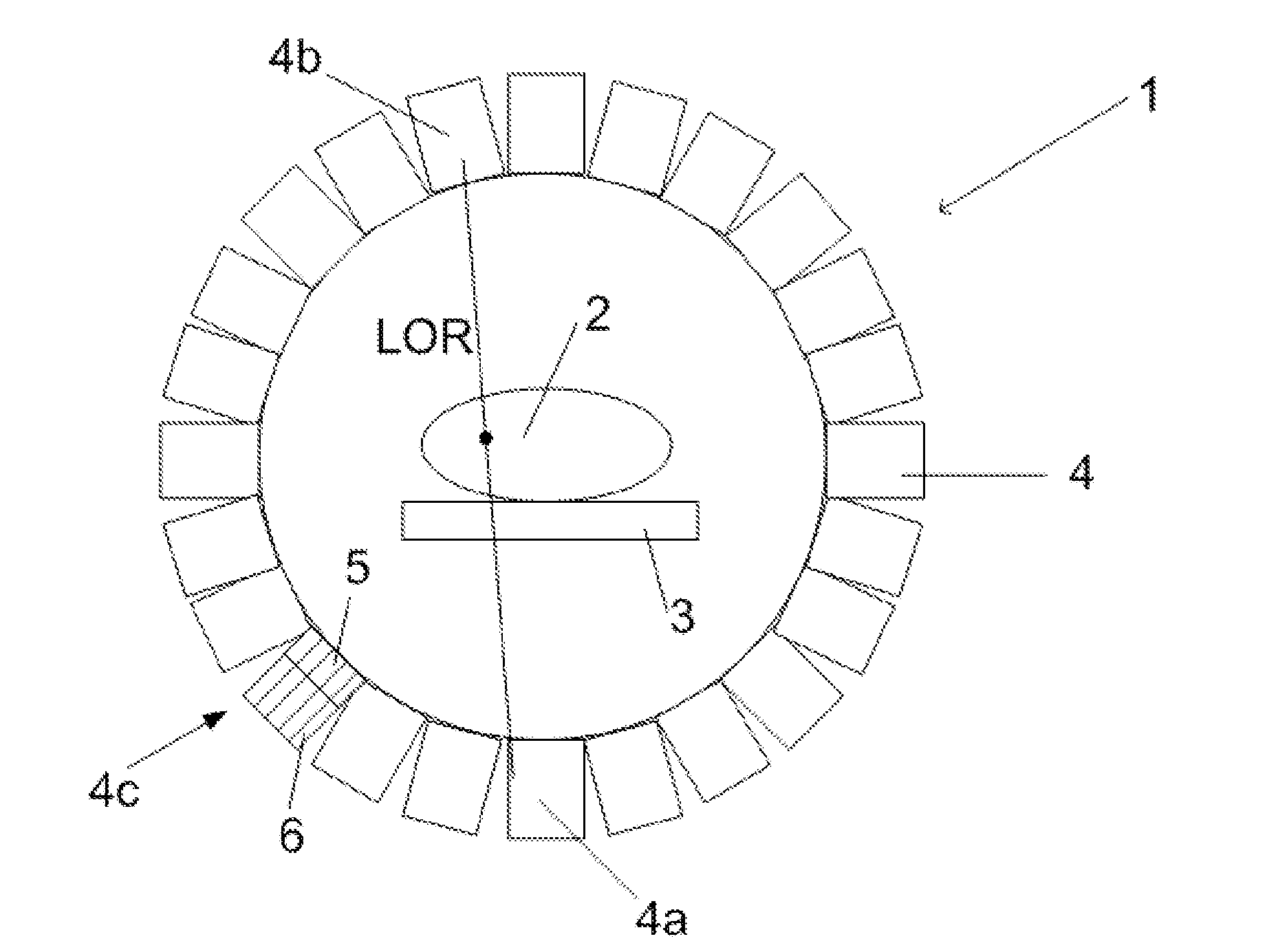
[0061]In the following, a preferred embodiment of the device for detecting highly energetic photons according to the invention will be described. Next, preferred embodiments of a module (comprising a plurality of these devices), a system (comprising a plurality of modules), a PET scanner, a gamma camera and a Compton camera according to the invention will be described.

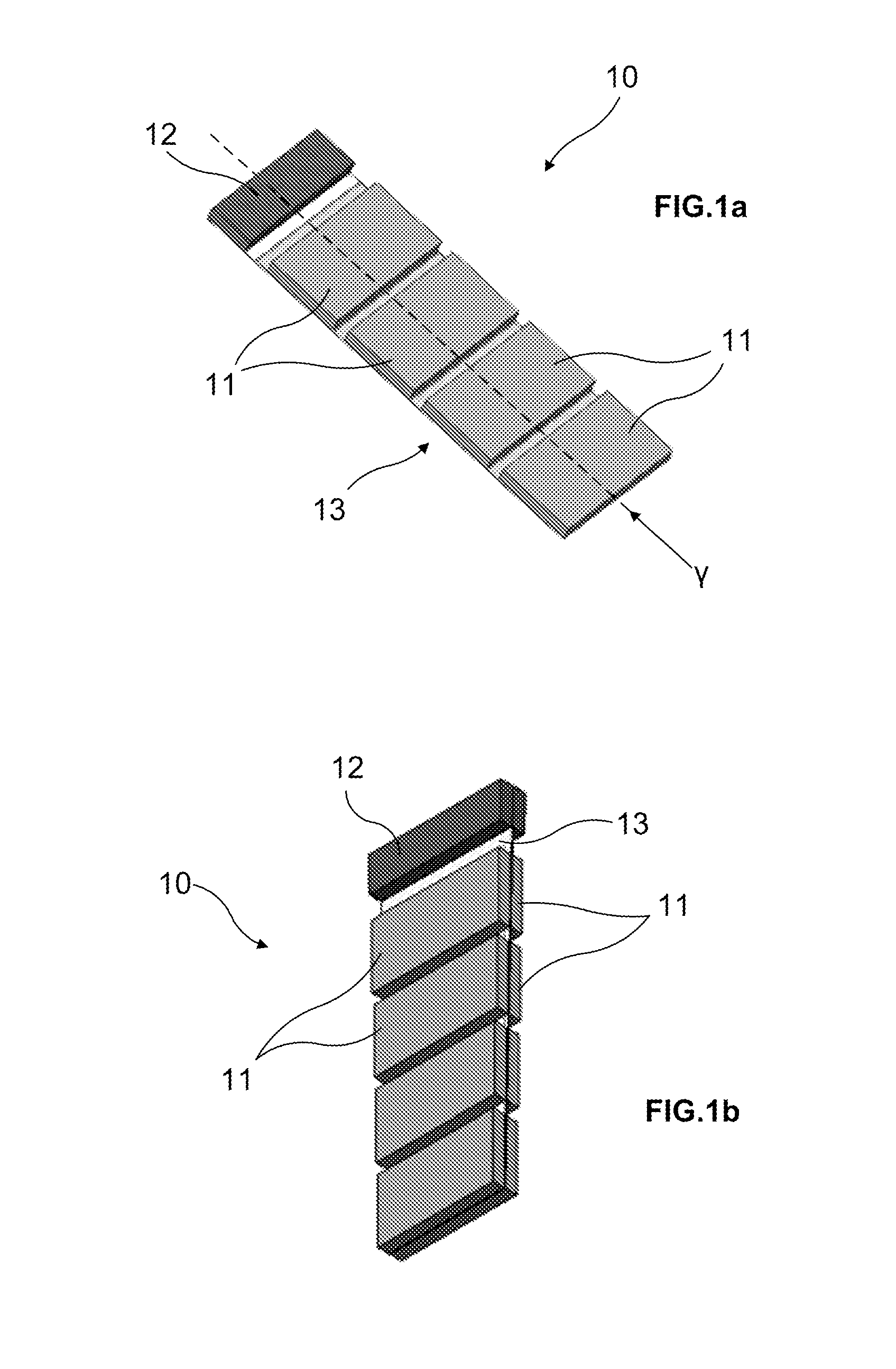
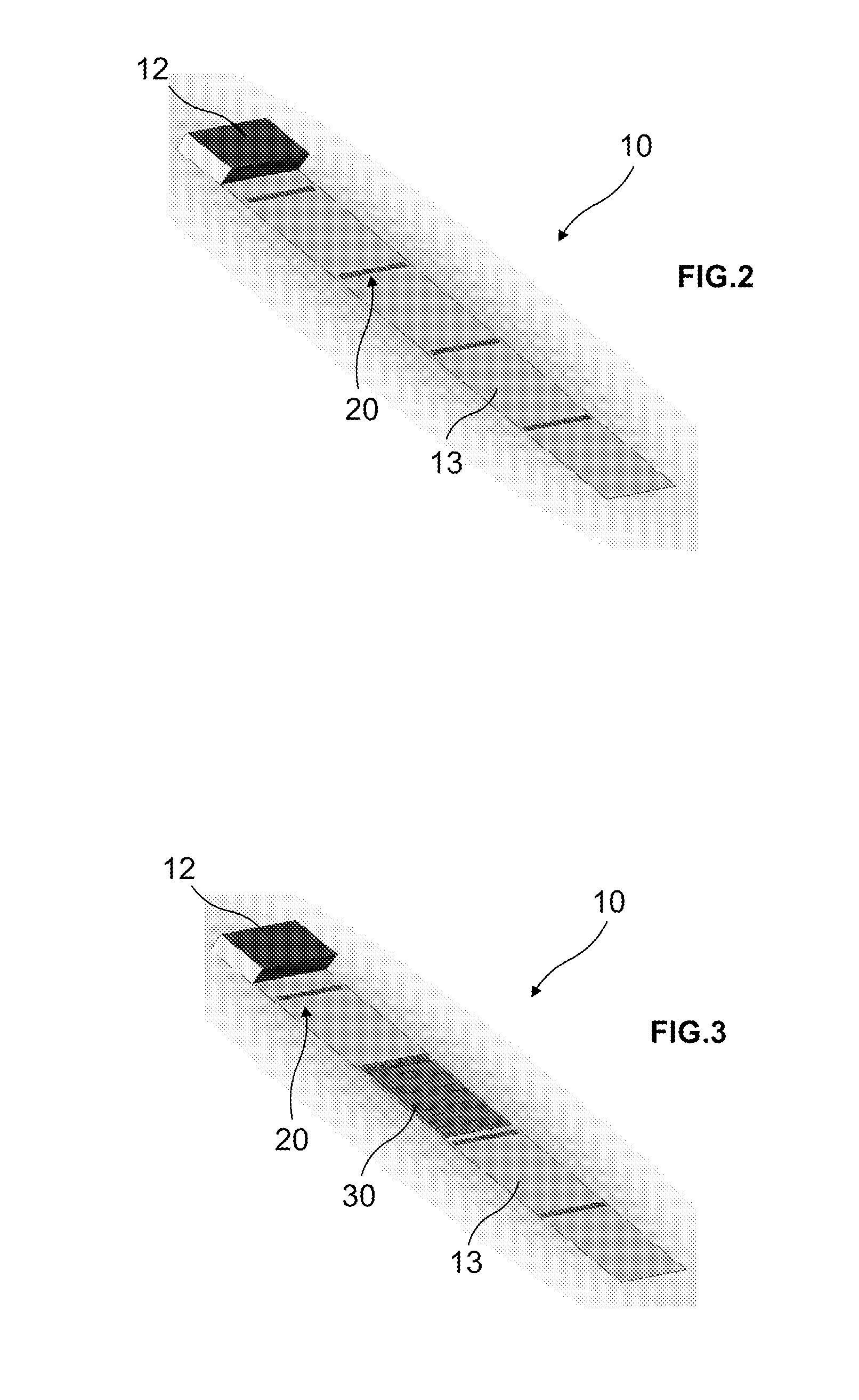
[0062]In FIG. 1a, a preferred embodiment of a device according to the present invention is shown. The device 10 for detecting highly energetic photons comprises four modular pixelated room temperature solid-state detectors 11 in a tiled / stacked scheme; four ASICs (application-specific integrated circuit), one for each solid-state detector 11, acting as readout elements for them; an input / output element connector 12 connected to the ASICs for data input and output (that is, mainly for obtaining the values generated by the ASICs from the solid-state detector captured parameters); and a kapton layer 13 acting as a base la...


PUM


Abstract

A device (10) for detecting highly energetic photons, comprising one or more pixelated solid-state detectors (11) for detecting the highly energetic photons; means for providing a high voltage for polarizing said solid-state detectors; one or more pixelated readout elements (30), a readout element being connected to each of said one or more pixelated solid-state detectors (11); an input / output element (12) connected to said readout elements (30) for data input and output; and a base layer (13) for mounting the pixelated solid-state detectors (11), the readout elements (30) and the input / output element (12).

Description

[0001]The present invention relates to a device for detecting highly energetic photons. More specifically, the invention relates to a device comprising pixelated room temperature solid-state detectors that detect gamma ray photons, generated by radioactive material inside a patient's body.[0002]The invention finds particular use in medical diagnostic imaging apparatus.BACKGROUND ART[0003]The Positron Emission Tomography (PET) is a diagnostic technique that obtains images that show the metabolism and functioning of tissues and organs (for example, the central nervous system).[0004]Like other diagnostic techniques in Nuclear Medicine, PET is based in detecting and analyzing the distribution inside the body of radioisotopes which have previously been administered to a patient. The radioisotopes may be taken in orally, they may be inhaled as gas or may be administered through an injection.[0005]Several positron-emitting radioisotopes for medical use are known. The most commonly used is ...

Claims


Application Information

Patent Timeline
Patent Type & Authority Applications(United States)
IPC IPC(8): G01T1/24
CPCG01T1/249G01T1/243G01T1/242
Inventor CHMEISSANI RAAD, MOKHTARLVAREZ PASTOR, JOSE M.SANCHEZ SANCHEZ, CARLOS
Owner INST DE FISICA D ALTES ENERTIES (IFAE)
Why Eureka
Try Eureka