
Method for manufacturing a silicon wafer

a manufacturing method and silicon wafer technology, applied in the field of silicon wafers, can solve the problems of increasing the leakage current in the manufactured device, increasing the complexity or advance of the technique for removing or capturing metal elements, and breaking wires, and achieves the effect of increasing the carbon density

Inactive Publication Date: 2011-10-27
SUMCO CORP
View PDF8 Cites 12 Cited by
  • Summary
  • Abstract
  • Description
  • Claims
  • Application Information

AI Technical Summary

Benefits of technology

[0015]A first object of the present invention is to provide a silicon wafer which does not have defects caused by crystal and which is low in the contamination degree by metal such as iron and excellent in electric characteristics, and provide a method for manufacturing the same.
[0016]A second object of the present invention is to provide a silicon wafer which has little agglomerates of point defects even if an ingot is pulled at a comparatively high speed and at a V / G value within a wide range, makes it possible to manufacture a semiconductor integrated circuit at a high yield rate and can be compatible with an existing device process thanks to its resistivity of 1 to 15 Ωcm and to provide a method for manufacturing the same.
[0017]A third object of the present invention is to provide a silicon wafer which can be adjusted so as to have a desired resistivity and a method for manufacturing the same.

Problems solved by technology

Above all among metal elements in a single crystal silicon, an iron element is thought to have a bad influence and this iron element is taken in by contamination from an environment or an apparatus.
In case that a large amount of metal element is mixed into a single crystal silicon ingot grown by the CZ method, however, it is necessary to more and more complicate or advance a technique for removing or capturing the metal element from a silicon wafer.
The OSF is made by a fact that a microscopic defect to be the nucleus of a crystal is introduced when growing the crystal, is actualized in a thermal oxidation process and the like when manufacturing a semiconductor device, and causes a failure such as the increase of leakage current in a manufactured device.
And existence of COPs on the surface of a wafer makes a step in a wiring process of a device and can cause breaking of wire.
And it may cause leakage and the like in an isolation part of a device and reduces the yield rate of a product.
When a wafer having an insufficient gettering ability is contaminated by metal in a device process, a defective operation of a device is caused by a junction leakage or a trap state by a metal impurity and thereby the yield rate of the product is lowered.
However, in a wafer being comparatively low in vacancy point defect density among silicon wafers composed of said perfect domain [P], oxygen precipitation does not always occur uniformly in the wafer in heat treatment in a device process and thereby the wafer sometimes cannot obtain a sufficient gettering effect.
And in case that the temperature gradient is constant, the value of V / G for producing a silicon wafer composed of a perfect domain [P] is in proportion to the pulling speed V of an ingot and it is required to pull the ingot at a comparatively low speed controlled within a narrow range, but it is not always technically easy to meet securely this requirement and the productivity of such an ingot also is not high.

Method used


Image

  • Method for manufacturing a silicon wafer
  • Method for manufacturing a silicon wafer
  • Method for manufacturing a silicon wafer

Examples


first embodiment

[A] First Embodiment of the Invention

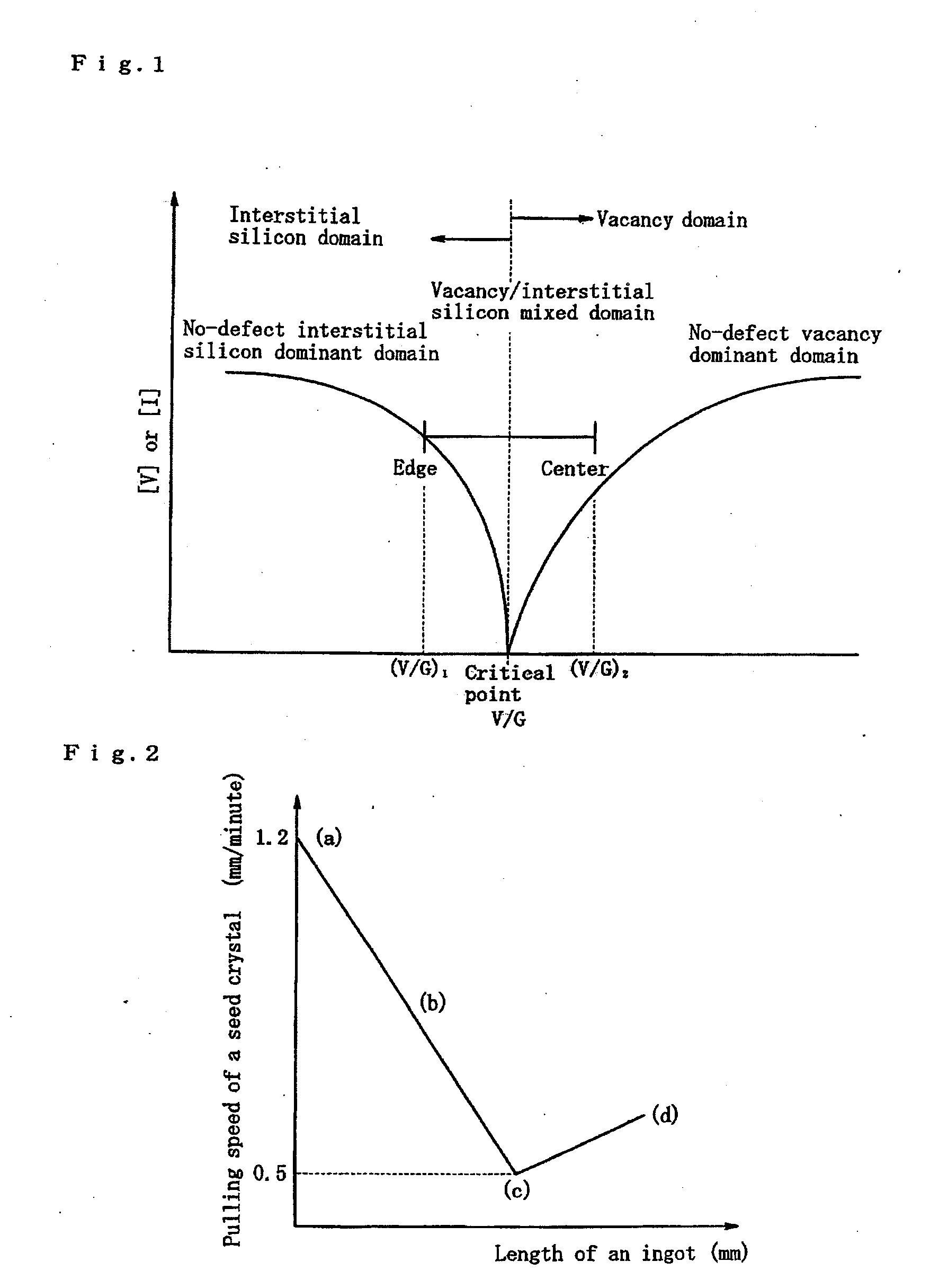
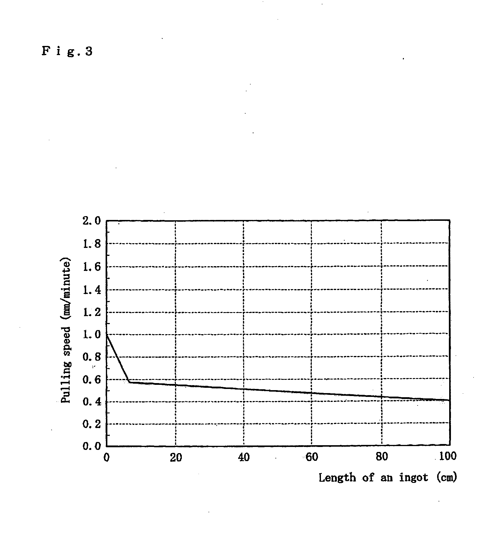
[0047]A silicon wafer according to first to third embodiments of the present invention is made by pulling an ingot at a specified pulling speed profile based upon Voronkov theory from a molten silicon liquid inside a hot zone furnace by the CZ method and then slicing this ingot.

[0048]A method for manufacturing a single crystal silicon ingot containing less amount of metal element and having no defect according to the first embodiment of the present invention is described.

(1) Method for Manufacturing a Single Crystal Silicon Containing Less Amount of Metal Element

[0049]A method for manufacturing a single crystal silicon ingot according to the first embodiment of the present invention, said ingot containing less amount of metal particularly iron, comprises a process of cleaning block-shaped or grain-shaped polycrystalline silicon to be raw material, a single crystal silicon pulling process of melting the cleaned material silicon and growing a singl...

second embodiment

[B] Second Embodiment of the Invention

[0068]A silicon wafer of a second embodiment of the present invention is made by pulling an ingot under a specified condition from a molten silicon liquid inside a hot zone furnace by means of the CZ method in the same way as the first embodiment and then slicing this ingot.

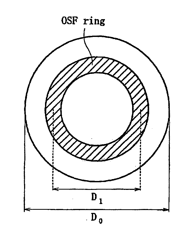
[0069]As described above, this CZ silicon wafer sometimes has OSF in the shape of a ring when it receives a thermal oxidation process. This OSF ring expands toward the outer circumference as the V / G value increases, and reduces its ring diameter and becomes disk-shaped in the center of the wafer and then disappears as the V / G value decreases.

[0070]This fact is described with reference to FIG. 9A. FIG. 9A shows a vertical section of an ingot obtained by gradually reducing the pulling speed and continuously decreasing the value of V / G. This ingot has been pulled as being doped with boron at a density of 1×10¹⁵ atoms / cm3 so that its conduction type is a p type and its resistivit...

third embodiment

[C] Third Embodiment of the Invention

[0083]A silicon wafer of a third embodiment of the present invention is made by pulling an ingot under a specified condition from a molten silicon liquid inside a hot zone furnace by means of the CZ method in the same way as the first embodiment and then slicing this ingot.

[0084]FIG. 13 is a characteristic diagram corresponding to FIG. 1 of the first embodiment. Here, it is described that there is a domain ((V / G)2 to (V / G)3) for forming an OSF nucleus in a domain [V] adjacent to a domain [P] and that a perfect domain [P] is further classified into a domain [P1] and a domain [PV]. This domain ((V / G)2 to (V / G)3) is a small domain of a domain in which vacancy point defects dominantly exist, said small domain being adjacent to a perfect domain, and is a domain in which no COP nor L / D is generated in the wafer. Domain [P1] is a domain where the ratio of V / G ranges from said (V / G)1 to the critical point, and domain [PV] is a domain where the ratio of V...


PUM

PropertyMeasurementUnit
thicknessaaaaaaaaaa
depthaaaaaaaaaa
resistivityaaaaaaaaaa

Abstract

Method for manufacturing a silicon wafer free of point defect agglomerates by processes including adding pure carbon to raw material of polycrystalline silicon, melting to become a molten silicon liquid, pulling a single silicon crystal ingot comprising a perfect domain [P] from the molten silicon liquid by controlling a ratio of V / G (mm2 / minute ° C.), lapping a silicon wafer cut out from the ingot, beveling the silicon wafer, chemical etching the beveled wafer so as to be removed damages of a surface of the wafer, and mirror-polishing the etched wafer, and the pure carbon is added to the raw material of polycrystalline silicon so that a density of carbon in the ingot becomes 1×10¹⁵ to 5×10¹⁵ atoms / cm3.

Description

CROSS-REFERENCE TO RELATED APPLICATIONS[0001]This application is a continuation of application Ser. No. 09 / 718,659, filed Nov. 22, 2000, the disclosure of which is incorporated by reference herein in its entirety.BACKGROUND OF THE INVENTION[0002]1. Field of the Invention[0003]The present invention relates to a silicon wafer made of a single crystal silicon ingot grown by the Czochralski method (hereinafter, referred to as CZ method) and a method for manufacturing the same wafer. And it relates more particularly to a silicon wafer to be used for manufacturing a semiconductor device such as an LSI and the like.[0004]2. Description of the Related Art[0005]A semiconductor device such as an LSI and the like needs to exhibit such excellent electric characteristics that a leakage current is a little in a pn junction and an MOS transistor has a high reliability in a gate oxide film. Crystal defects in a silicon wafer to be a substrate and contamination caused by a metal element in the wafer...

Claims


Application Information

Patent Timeline
Patent Type & Authority Applications(United States)
IPC IPC(8): H01L21/306
CPCC30B15/203C30B35/007C30B29/06
Inventor HARADA, KAZUHIROFURUYA, HISASHIMUROI, YUKIO
Owner SUMCO CORP
Learn More