
Nitride semiconductor device and manufacturing method of the device

Active Publication Date: 2011-12-22
PANASONIC CORP
View PDF7 Cites 28 Cited by
  • Summary
  • Abstract
  • Description
  • Claims
  • Application Information

AI Technical Summary

Benefits of technology

[0008]With this structure, an excellent p-type nitride semiconductor layer with high hole concentration of 1018 cm−3 or more is obtained without using annealing for activating p-type impurities, which has been conventionally required. Also, since there is no need to process a substrate, the number of steps decreases so that the device can be manufactured at low costs.
[0034]As compared to a conventional p-type nitride semiconductor layer obtained by implanting Mg into a nitride semiconductor layer and performing annealing, the present disclosure provides an excellent p-type nitride semiconductor layer with a high carrier concentration. Since the p-type nitride semiconductor layer with the high carrier concentration can be obtained without using annealing for activating p-type impurities, the number of steps decreases to significantly reduce costs. When the p-type nitride semiconductor layer obtained in this manner is used in the structure of, for example, a light-emitting device, a light-emitting device with a lower forward voltage (Vf) than a conventional device can be provided. Furthermore, since the p-type nitride semiconductor layer with the high carrier concentration can be obtained without using Mg, impurity diffusion into the light-emitting layer can be reduced, thereby enabling highly efficient light emitting.

Problems solved by technology

Also, when annealing is needed, the number of steps increases to increase manufacturing costs.
Furthermore, there is the problem that implanted Mg is diffused to a light-emitting layer.
When Mg is diffused, a crystal defect occurs in the light-emitting layer, thereby reducing internal quantum efficiency to significantly reduce luminous efficiency.
However, conditions for growth on the C-plane (0001) cannot be utilized.
Also, at present, a substrate formed by processing an off-substrate, of which the (001) plane of Si is inclined at an angle of 7°, to have unevenness needs to be used to increase the number of steps, thereby increasing manufacturing costs.

Method used


Image

  • Nitride semiconductor device and manufacturing method of the device
  • Nitride semiconductor device and manufacturing method of the device
  • Nitride semiconductor device and manufacturing method of the device

Examples


first exemplary embodiment

Manufacturing Method of First Exemplary Embodiment

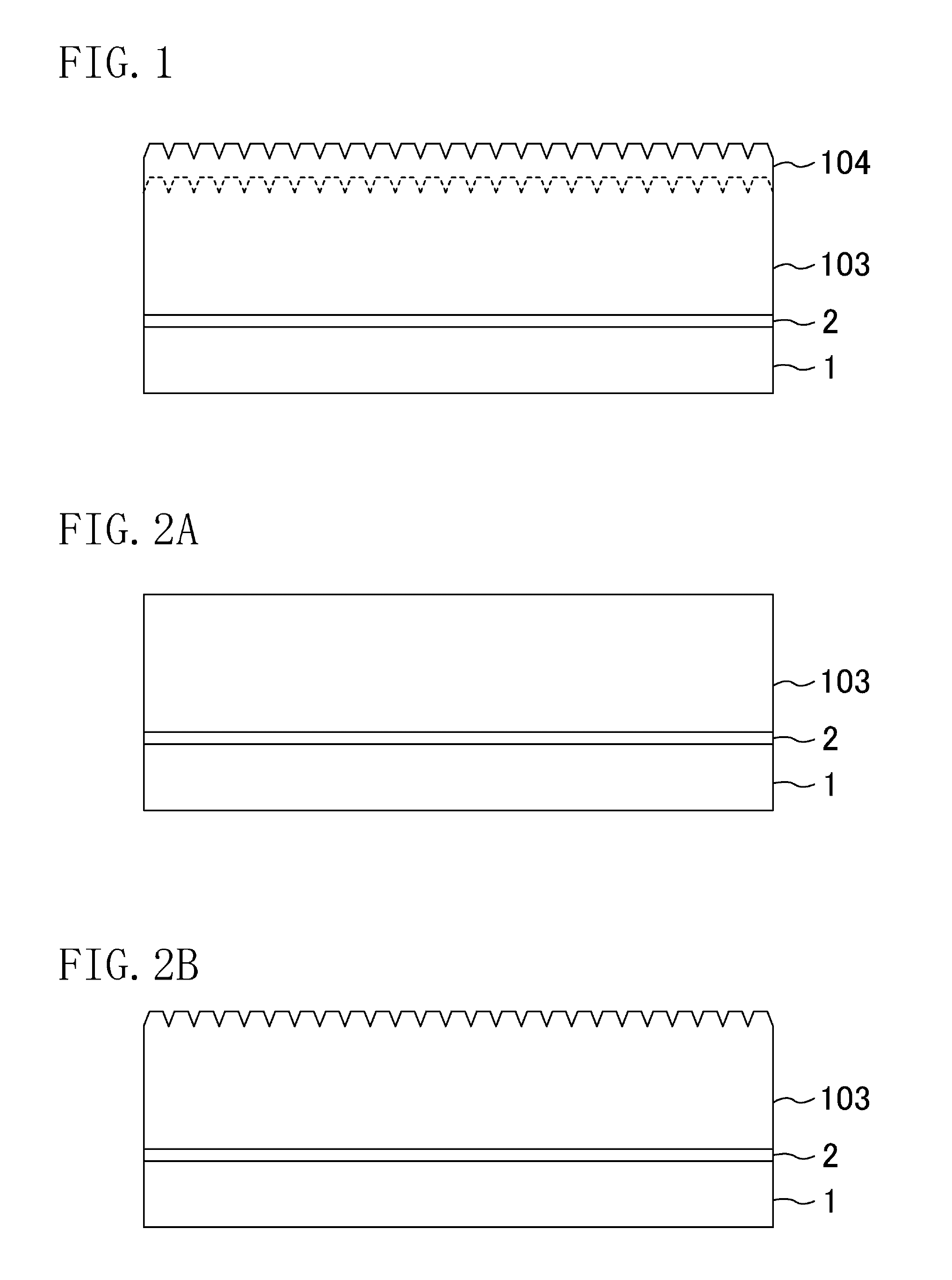
[0069]A manufacturing method of the LED of FIG. 1 will be described below. FIGS. 2A-2E illustrate the manufacturing method of the LED according to the first exemplary embodiment of the present disclosure.

[0070]A vapor deposition system such as metal-organic chemical vapor deposition (MOCVD), thermal CVD, halide vapor phase epitaxy (HDVPE), molecular beam epitaxy (MBE), or metal-organic molecular beam epitaxy (MOMBE) is used for crystal growth of the nitride semiconductor.

[0071]First, as shown in FIG. 2A, the buffer layer 2 made of AlN and the first nitride semiconductor layer 103 made of undoped GaN are formed in this order on the Si substrate 1 having the (111) plane as a principle surface, using the C-plane (0001) as a principle surface.

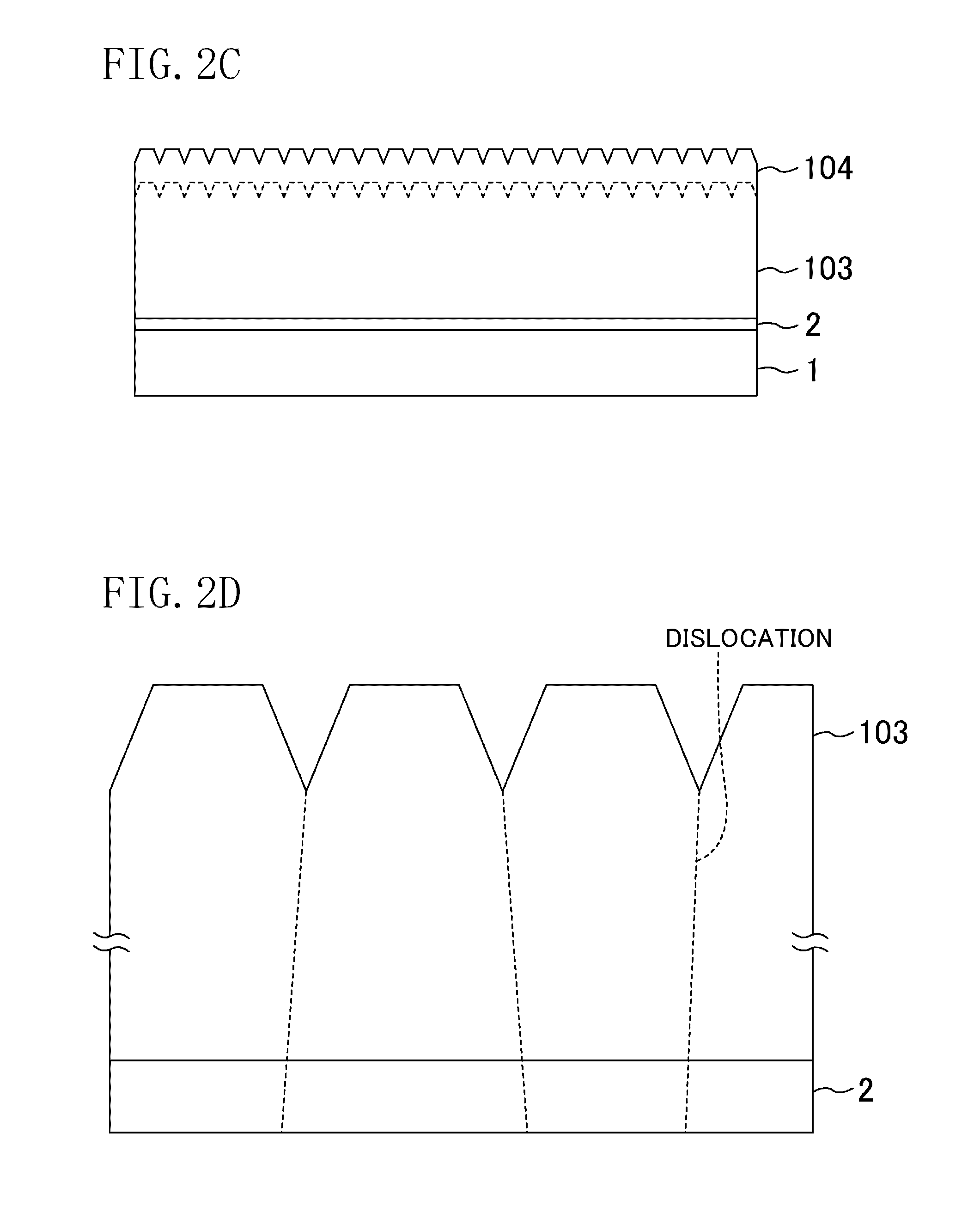
[0072]Next, as shown in FIG. 2B, unevenness is formed on the surface of the first nitride semiconductor layer 103. The unevenness is formed by, for example, crystal growth shown in FIG. 2D. Pit grow...

second exemplary embodiment

Second Variation of Second Exemplary Embodiment

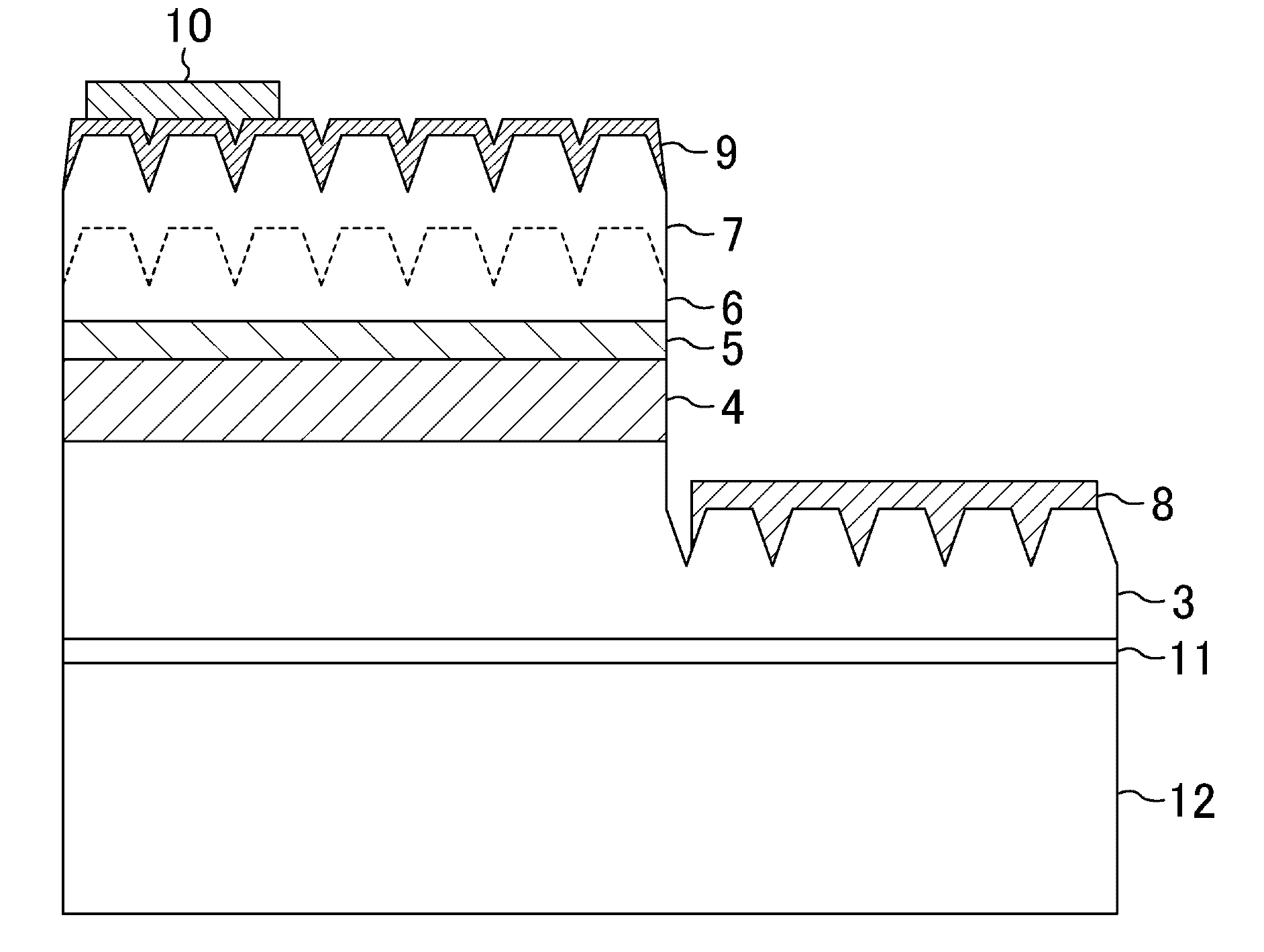
[0101]A second variation of the second exemplary embodiment of the present disclosure will be described below. While the LED shown in FIG. 3 has a so-called horizontal structure, the structure is not limited thereto and may be of a vertical type. FIG. 7 is a cross-sectional view of a vertical LED according to the second variation of the second exemplary embodiment. The same reference characters as those shown in the second exemplary embodiment are used to represent equivalent elements, and the explanation thereof will be omitted.

[0102]Differences from the second exemplary embodiment are as follows. In the second exemplary embodiment, parts of the second p-type nitride semiconductor layer 7, the first p-type nitride semiconductor layer 6, the OFS layer 5, and the light-emitting layer 4 are removed, and the negative electrode 8 is formed on the exposed surface of the n-type nitride semiconductor layer 3. On the other hand, the Si substrat...

third exemplary embodiment

[0104]A third exemplary embodiment will be described. While the LED has been described in the second exemplary embodiment, the p-type nitride semiconductor layer of the present disclosure is applicable to a laser diode (hereinafter referred to as an “LD”). FIG. 8 is a cross-sectional view of a laser diode according to the third exemplary embodiment of the present disclosure.

[0105]In the nitride semiconductor light-emitting device of the third exemplary embodiment, an n-type nitride semiconductor layer 203 made of n-type AlaGa1-aN, where 0204, an OFS layer 205 made of p-type AlGaN, the first p-type nitride semiconductor layer 6 made of p-type AlaGa1-aN, where 07 made of p-type AlaGa1-aN, where 0201 made of n-type and GaN having a (0001) plane as a principle surface, using the C-plane (0001) as a principle surface. In addition, a positive electrode 209 is formed on the second p-type nitride semiconductor layer 7, and a negative electrode 208 is formed on the back of the substrate 1, t...


PUM


Abstract

A nitride semiconductor device includes a first nitride semiconductor layer having a C-plane as a growth surface, and unevenness in an upper surface; and a second nitride semiconductor layer formed on the first nitride semiconductor layer to be in contact with the unevenness, and having p-type conductivity. The second nitride semiconductor layer located directly on a sidewall of the unevenness has a p-type carrier concentration of 1×10¹⁸ / cm3 or more.

Description

CROSS-REFERENCE TO RELATED APPLICATION[0001]This is a continuation of PCT International Application PCT / JP2010 / 000996 filed on Feb. 17, 2010, which claims priority to Japanese Patent Application No. 2009-050746 filed on Mar. 4, 2009. The disclosures of these applications including the specifications, the drawings, and the claims are hereby incorporated by reference in their entirety.BACKGROUND[0002]The present disclosure relates to p-type nitride semiconductor layers applicable to semiconductor devices such as light-emitting diodes and semiconductor lasers and manufacturing methods of the layers, and nitride semiconductor devices using the p-type nitride semiconductor layers and manufacturing method of the devices.[0003]So-called nitride semiconductor made of GaN, InN, AlN, and an alloy crystal of the materials has a band gap corresponding to the wavelength region ranging from a visible region to an ultraviolet region. The nitride semiconductor is a material which realizes a high-ou...

Claims


Application Information

Patent Timeline
IPC IPC(8): H01L33/26H01L21/20H01L29/12
CPCH01L21/0237H01L21/02381H01L21/0243H01L21/02433H01L21/02458H01L21/02494H01L33/32H01L21/02507H01L21/02516H01L21/0254H01L21/02579H01L21/0262H01L33/22H01L21/02502
Inventor FUKUSHIMA, YASUYUKIUEDA, TETSUZO
Owner PANASONIC CORP
Learn More