Supercharge Your Innovation With Domain-Expert AI Agents!

Material for organic photoelectric device, and organic photoelectric device thereby

a photoelectric device and organic technology, applied in triarylamine dyes, anthracene dyes, other domestic articles, etc., can solve the problems of limit in luminous efficiency, and achieve the effects of high efficiency, good hole and electron transporting properties, and thermal stability

Inactive Publication Date: 2012-01-19
CHEIL IND INC
View PDF1 Cites 4 Cited by
  • Summary
  • Abstract
  • Description
  • Claims
  • Application Information

AI Technical Summary

Benefits of technology

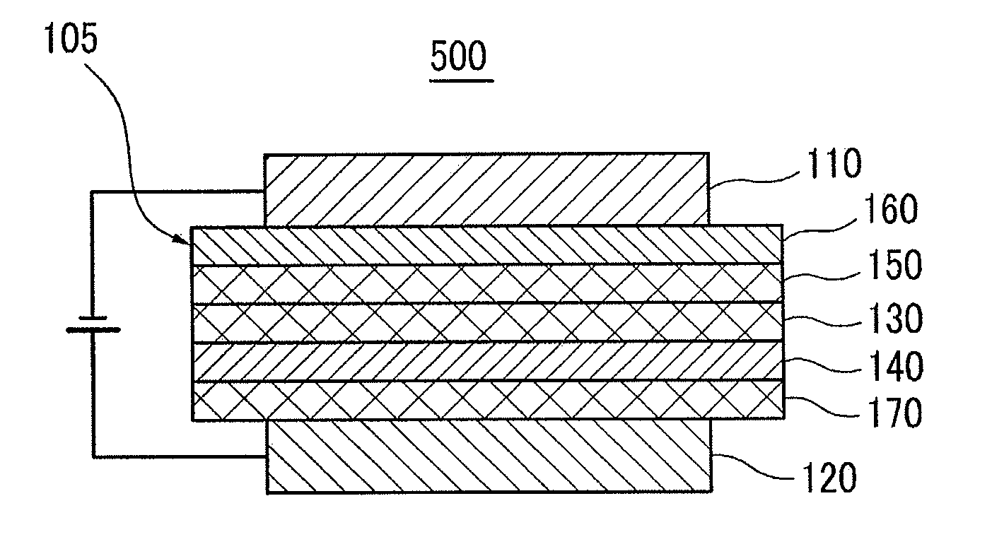
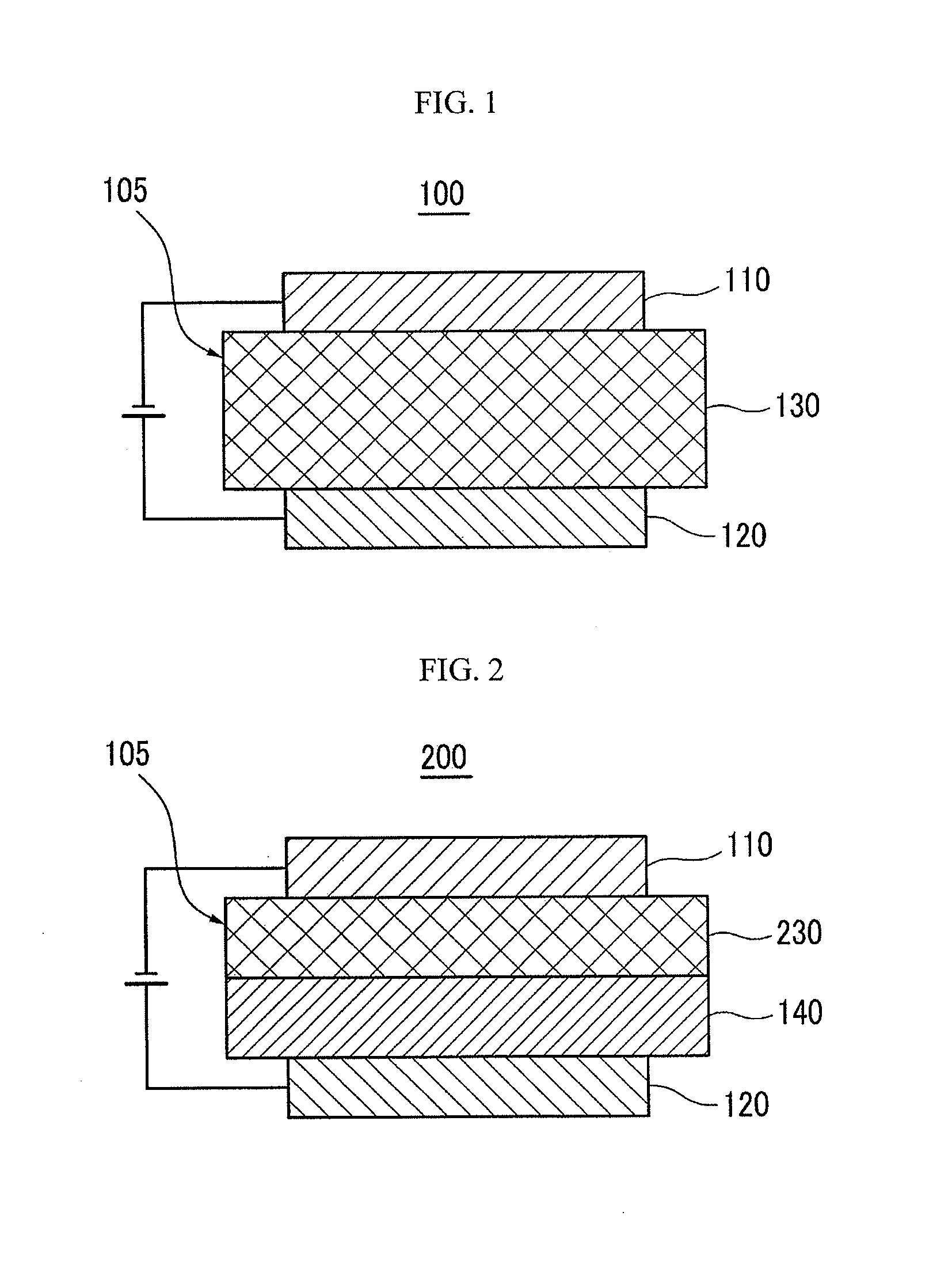
The patent text describes a material for an organic photoelectric device that has improved thermal stability and hole and electron transporting properties, resulting in a high efficiency device. The material includes a compound represented by Chemical Formula 1, which has good thermal stability and hole and electron transporting properties. The compound can be represented by Chemical Formula 2, wherein the substituents have different properties. The material can be used in an organic photoelectric device, providing better performance and stability.

Problems solved by technology

Accordingly, the percentage of the singlet exited state is 25% (the triplet is 75%) in the case of a fluorescent material, so it has limits in luminous efficiency.

Method used


Image

  • Material for organic photoelectric device, and organic photoelectric device thereby
  • Material for organic photoelectric device, and organic photoelectric device thereby
  • Material for organic photoelectric device, and organic photoelectric device thereby

Examples


example 1

Synthesis of Material for Organic Photoelectric Device

example 1-1

Synthesis of Compound (16)

[0152]The following compound (16) was synthesized as shown in the following Reaction Scheme 1.

[0153]Step 1: Synthesis of Intermediate Product (A)

[0154]40.4 g (241 mmol) of carbazole, 38.0 g (121 mmol) of 1,3,5-tribromobenzene, 2.99 g (30 mmol) of cuprous chloride, and 66.7 g (483 mmol) of potassium carbonate were suspended in 171 ml of dimethylsulfoxide, and refluxed under a nitrogen atmosphere for 8 hours while heating.

[0155]The refluxed reaction solution was cooled to room temperature and recrystallized with methanol. The precipitated crystals were separated by filtration and the obtained residue was purified by silica gel column chromatography, providing 36.7 g of the first crystalline intermediate (A) (yield 62.4%).

[0156]Step 2: Synthesis of Intermediate Product (B)

[0157]35.0 g (72 mmol) of intermediate product (A) was dissolved in 350 ml of tetrahydrofuran, and then 61.5 ml (98 mmol) of n-butyl lithium hexane solution (1.6 M) was added thereto under an...

example 1-2

Synthesis of Compound (24)

[0170]The following compound (24) was synthesized as shown in the following Reaction Scheme 2.

[0171]Step 1: Synthesis of Intermediate Product (F)

[0172]15 g (63 mmol) of 1,3-dibromobenzene, 7.66 g (44 mmol) of 1-naphthalene boronic acid, 17.58 g (127 mmol) of potassium carbonate, and 1.83 g (50 mmol) of tetrakis(triphenylphosphine)palladium were suspended in 200 ml of tetrahydrofuran, 200 ml of toluene, and 50 ml of purified water, and refluxed under a nitrogen atmosphere for 24 hours while heating.

[0173]The refluxed reaction solution was cooled to room temperature, and the reaction solution was separated into two layers. The solution obtained after the organic solvent of the organic layer was removed under a reduced pressure was separated using column chromatography (hexane), and then solvent was removed to obtain 15 g (83%) of a gel-type intermediate product (F).

[0174]Step 2: Synthesis of Intermediate Product (G)

[0175]7 g (24 mmol) of the intermediate prod...


PUM

PropertyMeasurementUnit
internal quantum efficiencyaaaaaaaaaa

Abstract

A material for an organic photoelectric device, the material including a compound represented by the following Chemical Formula 1:wherein, in Chemical Formula 1,HTU and HTU′ are independently hole transporting units, andR1 to R3 are independently a substituent selected from the group of hydrogen, a substituted or unsubstituted C6 to C30 aryl, a substituted or unsubstituted C2 to C30 heteroaryl, and a substituted or unsubstituted C1 to C30 alkyl,wherein the term “substituted” refers to one substituted with a halogen, a C1 to C30 alkyl, a C1 to C30 haloalkyl, a C6 to C30 aryl, a C2 to C30 heteroaryl, a C1 to C20 alkoxy, or combinations thereof.

Description

CROSS-REFERENCE TO RELATED APPLICATION[0001]This is a divisional application based on pending application Ser. No. 12 / 662,765, filed May 3, 2010, which in turn is a continuation of International Application No. PCT / KR2008 / 006452, entitled “Material for Organic Photoelectric Device, and Organic Photoelectric Device Thereby,” filed Oct. 31, 2008, the entire contents of both of which are hereby incorporated by reference.BACKGROUND[0002]1. Field[0003]Embodiments relate to a material for an organic photoelectric device, and an organic photoelectric device using the same.[0004]2. Description of the Related Art[0005]A photoelectric device is, in a broad sense, a device for transforming photo energy to electrical energy, and conversely, for transforming electrical energy to photo energy. The photoelectric device may be exemplified by an organic light emitting diode, a solar cell, a transistor, and so on.[0006]Particularly, among these photoelectric devices, the organic light emitting device...

Claims


Application Information

Patent Timeline
Patent Type & Authority Applications(United States)
IPC IPC(8): H01L51/54C07D401/14C07D401/10C07D213/38
CPCC07D213/38C09B1/00C09K11/06H01L51/006H01L51/0067H01L51/0072H01L51/0085H01L51/5016H01L51/5048H05B33/20H05B33/22Y10S428/917C09B57/00C09B57/001C09B57/008C07D401/14H10K85/633H10K85/654H10K85/6572H10K85/342H10K50/11H10K2101/10H10K50/14
Inventor KIM, YOUNG-HOONYU, EUN-SUNKIM, NAM-SOOCHAE, MI-YOUNG
Owner CHEIL IND INC
Features
  • R&D
  • Intellectual Property
  • Life Sciences
  • Materials
  • Tech Scout
  • Unparalleled Data Quality
  • Higher Quality Content
  • 60% Fewer Hallucinations
Learn More