
Silver conductive film and production method thereof

a technology of silver conductive film and production method, which is applied in the direction of conductive layers on insulating supports, liquid/solution decomposition chemical coating, transportation and packaging, etc., can solve the problem of difficulty in forming a texture directly

Inactive Publication Date: 2012-02-23
DOWA ELECTRONICS MATERIALS CO LTD
View PDF13 Cites 7 Cited by
  • Summary
  • Abstract
  • Description
  • Claims
  • Application Information

AI Technical Summary

Benefits of technology

The present invention provides a thin-film silver conductive film that can be used as the rear-surface electrode of a thin-film solar cell. This film has a low resistance and high reflectance, with a texture structure that improves the efficiency of the solar cell. The film can be produced in a non-vacuum atmosphere at lower temperatures, and has excellent adhesiveness to the substrate. The film has a dense structure with a small number of voids, and is mechanically stable. The film can be easily produced and has a low carbon content, which makes it suitable for use in flexible thin-film solar cells.

Problems solved by technology

However, in a thin-film solar cell, the thickness of the photoelectric conversion layer is, for example, at most 500 nm or so and is thin, and therefore it is difficult to form a texture directly in the incident plane of the cell, and accordingly in this, the transparent electrode adjacent to the light-receiving surface of the photoelectric conversion layer is roughened to have fine projections and recesses, thereby forming the intended texture therein.

Method used


Image

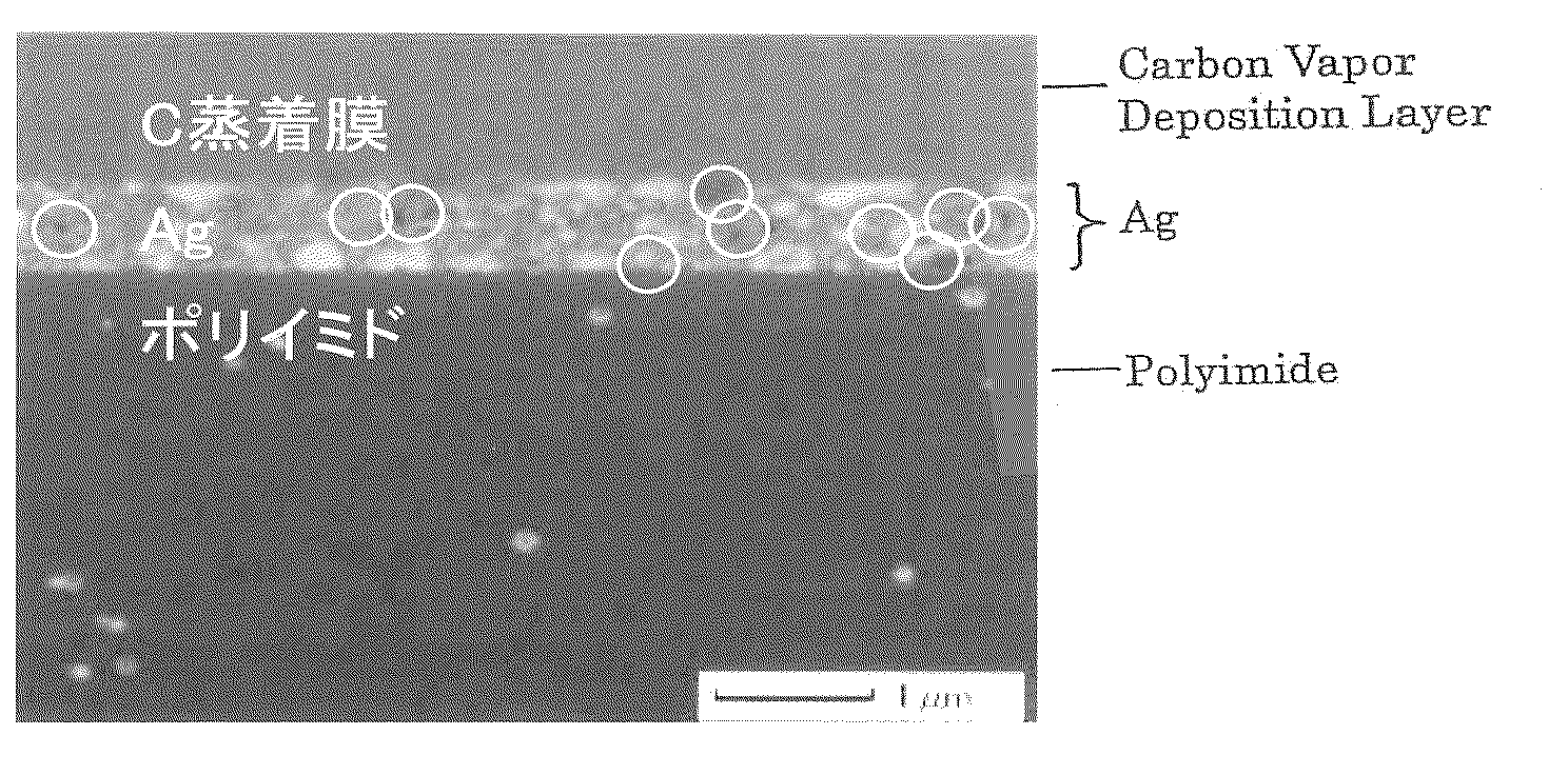
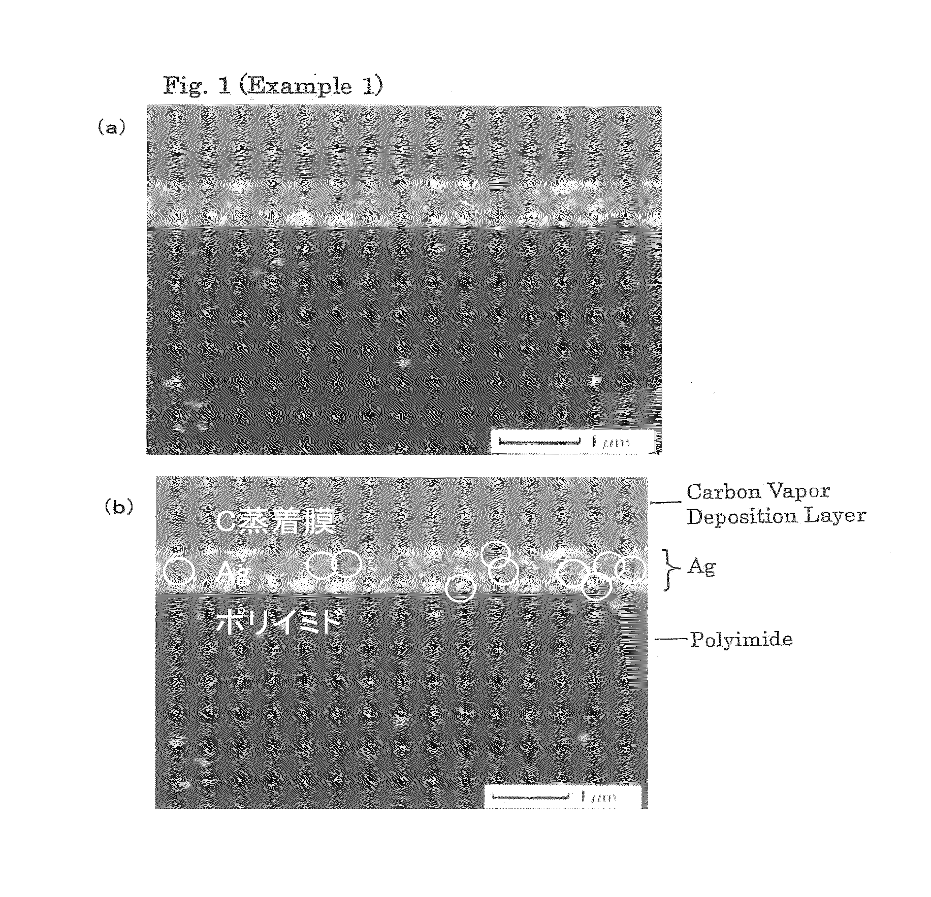
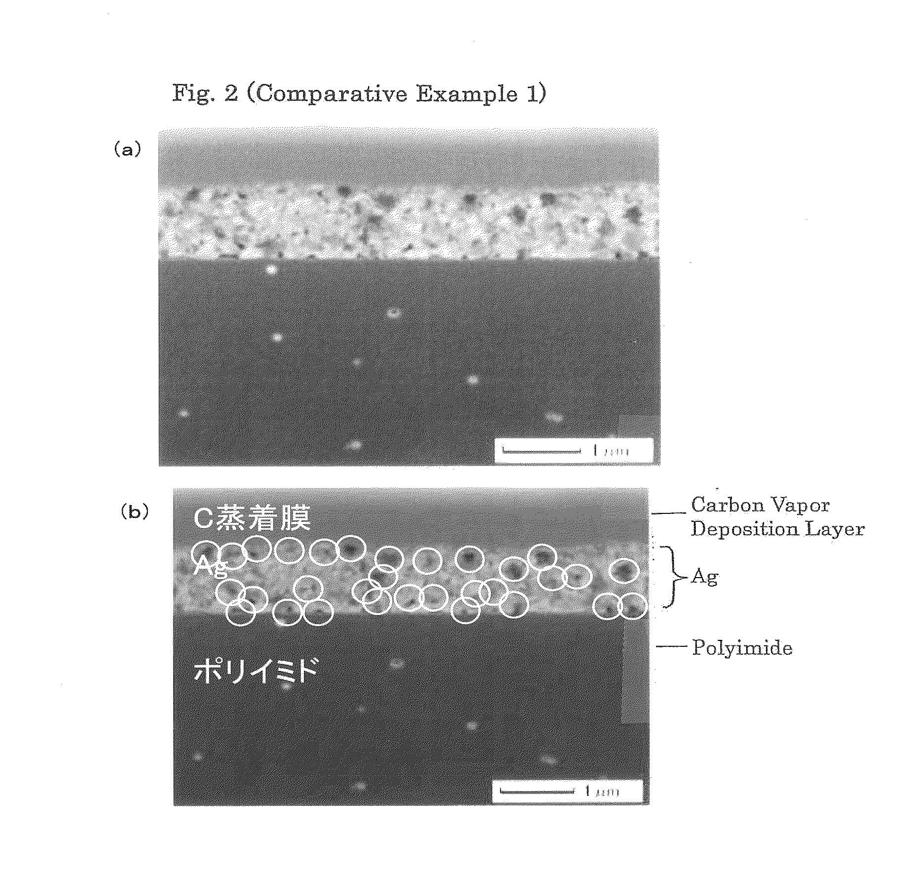
  • Silver conductive film and production method thereof
  • Silver conductive film and production method thereof
  • Silver conductive film and production method thereof

Examples


example 1

[0046]200 mL of isobutanol (Wako Pure Chemical's special grade chemical) serving both as a reaction medium and as a reducing agent, 27 mL of oleylamine (by Wako Pure Chemical, Mw=267) as an organic compound, and 13.7 g of silver nitrate crystal (by Kanto Chemical) as a silver compound were prepared, and these were mixed and stirred with a magnet stirrer to dissolve the silver nitrate.

[0047]The solution was transferred into a container equipped with a reflux condenser, and set in an oil bath. With a flow of nitrogen gas as an inert gas jetted into the container at a flow rate of 400 mL / min, the solution was heated with stirring with a magnet stirrer at a revolution speed of 100 rpm. The heating rate up to 100° C. was 2° C. / min. At a temperature of 100° C., this was refluxed for 3 hours, and then 8.5 g (molar ratio to Ag, 1.0) of a secondary amine, diethanolamine (by Wako Pure Chemical, Mw=106) as a reduction promoter was added to it. Next, this was kept as such for 1 hour, and the re...


PUM

PropertyMeasurementUnit
boiling pointaaaaaaaaaa
mean particle size DTEMaaaaaaaaaa
temperatureaaaaaaaaaa

Abstract

Provided is a silver conductive film, a thin film of silver comprising a sintered layer of silver particles having a mean particle size DTEM of at most 100 nm. Its specific resistance is at most 5 μΩ·cm, the ratio of the voids in the sintered layer is at most 3 / μm2, and the film has a texture structure with a surface roughness Ra of from 10 to 100 nm. The silver conductive film having such a texture structure may be produced according to a production process comprising a step of applying a silver particle dispersion of silver particles having a mean particle size DTEM of at most 100 nm dispersed in a non-polar or poorly-polar liquid organic medium having a boiling point of from 60 to 300° C., onto a substrate to form a coating film thereon, and thereafter baking the coating film.

Description

TECHNICAL FIELD[0001]The present invention relates to a silver conductive film suitable for the rear-surface, electrode-side conductive layer of a thin-film solar cell, and to a production method thereof.PRIOR ART[0002]A thin-film solar cell has a large light absorption coefficient in the photoelectric conversion layer thereof and has a high incident light utilization efficiency, as compared with a bulk-type solar cell, and is therefore advantageous in that the amount of the silicon material to be used may be reduced. In addition, it is further characterized in that its photoelectric conversion layer may be formed at a relatively low temperature and its environmental load is small.[0003]A solar cell effectively utilizes the incident light thereto, and therefore it is effective to form a texture structure in the incident plane thereby lowering the reflectance on the surface so as to reduce the loss by reflection. In a bulk-type solar cell, it is possible to form a texture structure d...

Claims


Application Information

Patent Timeline
Patent Type & Authority Applications(United States)
IPC IPC(8): B05D5/12B05D3/12B05D3/02B82Y40/00
CPCC23C18/08H01L31/022425Y10T428/24413Y02E10/50H01L31/0392H01B5/14H01B13/00H01L31/04
Inventor SATO, KIMITAKAHISAEDA, YUTAKAOKANO, TAKUOGI, KOZO
Owner DOWA ELECTRONICS MATERIALS CO LTD
Learn More