Compliant printed circuit peripheral lead semiconductor test socket

a technology of lead semiconductors and peripherals, which is applied in the direction of printed circuit manufacture, electrical apparatus construction details, instruments, etc., can solve the problems of affecting the performance affecting the reliability of the circuit board, etc., to achieve excellent electrical performance, reduce the cost of production, and reduce the effect of contact loss

Active Publication Date: 2012-03-01
HSIO TECH
View PDF2 Cites 60 Cited by
  • Summary
  • Abstract
  • Description
  • Claims
  • Application Information

AI Technical Summary

Benefits of technology

[0008]The present disclosure is aimed at a test socket that is inexpensive to produce, has relative long life and provides excellent electrical performance.

Problems solved by technology

A socket with good electrical performance is critical for many IC testing functions since poor performance can result in retesting or discarding devices that are actually acceptable but failed the test due to degradation within the socket.
In general, they all have a range of mechanical life that is limited by the effects of contacting the solder that is plated onto the terminals of the IC device.
As the solder collects on the tips of the contacts, the Tin within the solder oxidizes to form a high resistance layer that causes the contact to lose electrical performance.
This movement can cause wear on the PCB which can degrade performance of the circuit board.
In general, the need for thousands of cycles before replacement drives sophisticated design that can be expensive.
The socket volumes can also be relatively small requiring custom production methods that can also be expensive.
The methods used to produce the plastic socket housings which hold the contacts are typically expensive precision machining operations.
Those sockets that can pass the electrical performance requirements can be limited by cost or the amount of use before they must be repaired or replaced.
It can take hours or days to replace the failing socket, with the corresponding unit volume of IC devices which could have been tested being a major factor in the overall cost of use (e.g., an opportunity cost).
Damage to the PCB used for the test interface can also dramatically impact the cost of use as the PCB's can be very expensive and have a long lead-time to build (and replace).

Method used


Image

  • Compliant printed circuit peripheral lead semiconductor test socket
  • Compliant printed circuit peripheral lead semiconductor test socket
  • Compliant printed circuit peripheral lead semiconductor test socket

Examples


Embodiment Construction

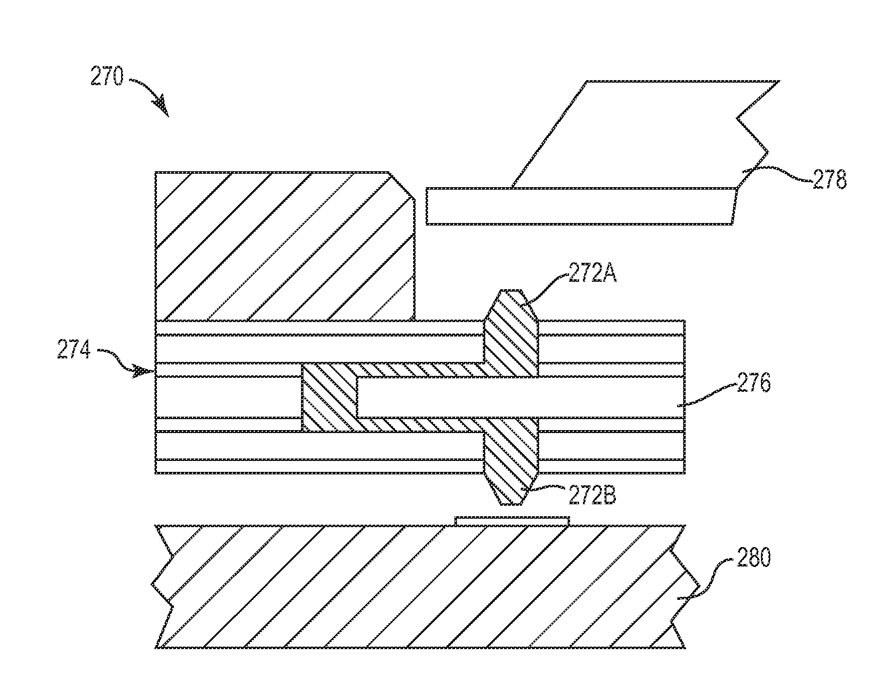
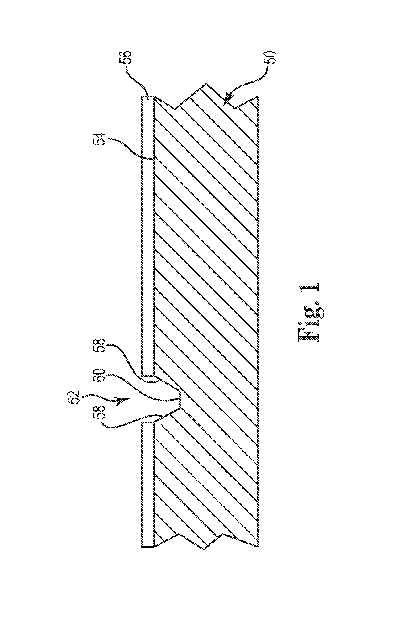
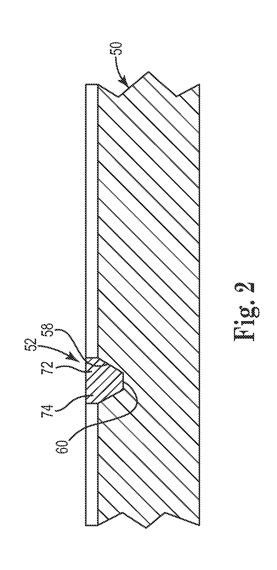
[0037]The present test sockets can be used to test semiconductor and other electrical devices having contact-to-contact spacing (pitch) on the order of less than about 1.0 millimeter (1×10⁻³ meter), and more preferably a pitch of less than about 0.7 millimeter, and most preferably a pitch of less than about 0.4 millimeter. Such fine pitch test sockets are especially useful for evaluating IC devices.

[0038]FIG. 1 is a side cross-sectional view of a fixture 50 useful in making a test socket in accordance with an embodiment of the present disclosure. The fixture 50 can include a plurality of cavities 52 (or recesses) in the first surface 54. The locations of the cavities 52 are arranged in an array that corresponds to terminals 62 on an IC device 64 (see FIG. 6). The cavities 52 can be formed using any of a variety of techniques, including but not limited to molding, machining, printing, imprinting, embossing, etching, coining, and the like.

[0039]In the illustrated embodiment, the cavit...


PUM

PropertyMeasurementUnit
widthaaaaaaaaaa
aspect ratioaaaaaaaaaa
conductiveaaaaaaaaaa

Abstract

A test socket that provides a temporary interconnect between terminals on an integrated circuit (IC) device and contact pads on a test printed circuit board (PCB). The test socket includes a compliant printed circuit and a socket housing. The compliant printed circuit includes at least one compliant layer, a plurality of first contact members located along a first major surface, a plurality of second contact members located along a second major surface, and a plurality of conductive traces electrically coupling the first and second contact members. The compliant layer is positioned to bias the first contact members against the terminals on the IC device and the second contact members against contact pads on the test PCB. The socket housing is coupled to the compliant printed circuit so the first contact members are positioned in a recess of the socket housing sized to receive the IC device.

Description

FIELD OF THE INVENTION[0001]The present disclosure relates to a high performance electrical interconnect between an integrated circuit and a printed circuit assembly, and in particular, to a peripheral lead semiconductor test socket.BACKGROUND OF THE INVENTION[0002]Traditional peripheral lead integrated circuit (IC) test sockets are generally constructed of a machined engineering grade plastic housing and frame, which is populated with a series of contact members that correspond to the terminals on two or four sides of the IC device. These contacts provide a temporary connection between the IC device terminals and the appropriate location on a test printed circuit board (PCB), also called a test or load board. This temporary electrical connection provides the mechanism to power the IC device and test performance.[0003]The IC devices are graded based upon performance, and the devices that pass are identified while the devices that fail are either retested or discarded. In many cases,...

Claims


Application Information

Patent Timeline
Patent Type & Authority Applications(United States)
IPC IPC(8): G01R31/00H05K3/00
CPCY10T29/49147Y10T29/49155G01R1/0483H05K7/1061Y10T29/49128Y10T29/49126G01R1/0466
Inventor RATHBURN, JAMES
Owner HSIO TECH
Why Eureka
Try Eureka