Memory device

Active Publication Date: 2012-03-15
SEMICON ENERGY LAB CO LTD
View PDF8 Cites 83 Cited by
  • Summary
  • Abstract
  • Description
  • Claims
  • Application Information

AI Technical Summary

Benefits of technology

[0005]Examples of a semiconductor memory device (hereinafter, simply referred to as a memory device) include a DRAM and an SRAM which are categorized as a volatile memory; a mask ROM, an EPROM, an EEPROM, a flash memory, and a ferroelectric memory which are categorized as a nonvolatile memory; and the like. Most of these memories including single crystal semiconductor substrates are already put into practical use. Among the above memory devices, a DRAM has a simple structure in which a memory cell includes a transistor and a capacitor and needs fewer semiconductor elements for forming a memory cell than other memory devices such as an SRAM. Therefore, memory capacity per unit area can be increased as compared to other memory devices, and thus, a DRAM is advantageous in cost reduction.

Problems solved by technology

Thus, if a slight amount of off-state current exists in the transistor, it is difficult to maintain the accuracy of data, and a holding period tends to be short.
Accordingly, frequency of refresh operation is increased and power consumption is increased.

Method used


Image

  • Memory device
  • Memory device
  • Memory device

Examples


embodiment 1

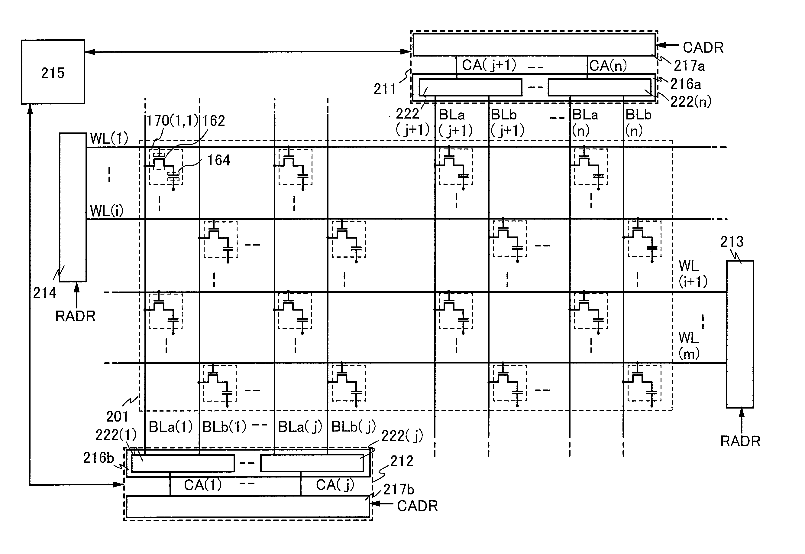
[0078]A structure of a memory device according to an embodiment of the present invention will be described with reference to FIG. 1, FIGS. 2A and 2B, FIGS. 3A to 3H, FIGS. 4A to 4C, FIG. 5, FIG. 6, FIG. 7, and FIG. 8.

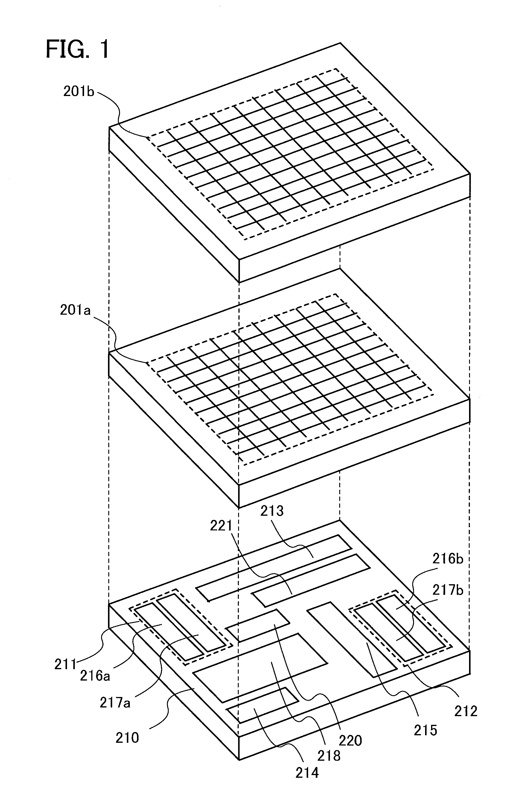
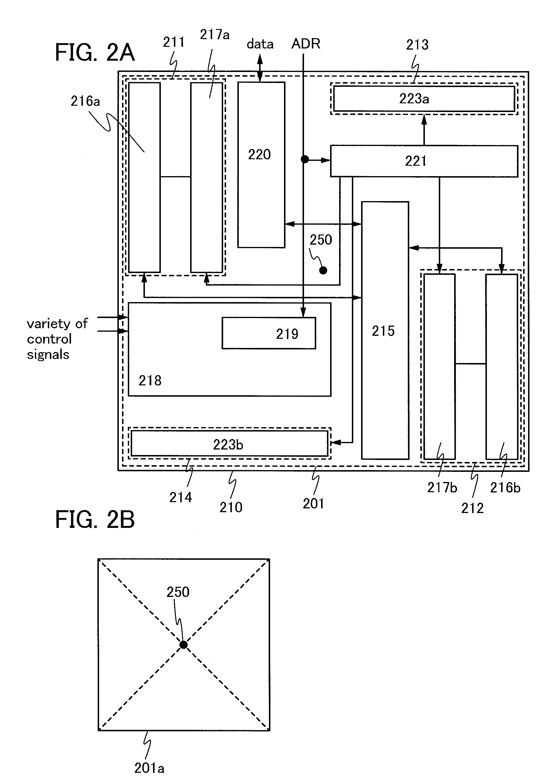
[0079]FIG. 1 is a schematic view illustrating an example of a structure of a memory device. The memory device according to an embodiment of the present invention has a stacked structure which includes a plurality of memory cell arrays (in FIG. 1, two memory cell arrays are typically illustrated) in the upper portion and a peripheral circuit including as a control circuit or a driver circuit which is required to operate at high speed for driving the plurality of memory cell arrays in the lower portion. Note that the driver circuit or the control circuit may include a logic circuit, an analog circuit, and / or an arithmetic circuit.

[0080]The memory device illustrated in FIG. 1 includes a memory cell array 201a including a plurality of memory cells and a memory cell array 20...

embodiment 2

[0151]In this embodiment, a structure and a manufacturing method of a memory device according to an embodiment of the present invention will be described with reference to FIGS. 9A and 9B, FIGS. 10A and 10B, FIGS. 11A and 11B, FIGS. 12A to 12D, FIGS. 13A to 13E, FIGS. 14A to 14D, and FIGS. 16A and 16B.

[0152]FIG. 9A and FIG. 16A are cross-sectional views of a memory device. In FIG. 9A, a cross section B1-B2 is parallel to the channel length direction of a transistor. In FIG. 16A, a cross section C1-C2 is parallel to the channel width direction of a transistor. The memory device illustrated in FIG. 9A and FIG. 16A includes the memory cell array 201a and the memory cell array 201b in the upper portion and the peripheral circuit 210 in the lower portion. A memory cell 170a included in the memory cell array 201a and a memory cell 170b included in the memory cell array 201b are illustrated as an example of the plurality of memory cells included in the memory cell array 201a and the memory...

embodiment 3

[0296]One embodiment of an oxide semiconductor layer which can be used for a channel formation region of the transistor 162 in the above embodiments will be described with reference to FIGS. 14A to 14D.

[0297]The oxide semiconductor layer of this embodiment has a stacked structure including a first crystalline oxide semiconductor layer and a second crystalline oxide semiconductor layer which is over the first crystalline oxide semiconductor layer and has a larger thickness than the first crystalline oxide semiconductor layer.

[0298]A first oxide semiconductor film with a thickness greater than or equal to 1 nm and less than or equal to 10 nm is formed over an insulating layer 140.

[0299]In this embodiment, an oxide insulating layer with a thickness greater than or equal to 50 nm and less than or equal to 600 nm is formed as the insulating layer 140 by a PCVD method or a sputtering method. For example, a single layer selected from a silicon oxide film, a gallium oxide film, an aluminum ...


PUM


Abstract

In a memory device, memory capacity per unit area is increased while a period in which data is held is ensured. The memory device includes a driver circuit provided over a substrate, and a plurality of memory cell arrays which are provided over the driver circuit and driven by the driver circuit. Each of the plurality of memory cell arrays includes a plurality of memory cells. Each of the plurality of memory cells includes a first transistor including a first gate electrode overlapping with an oxide semiconductor layer, and a capacitor including a source electrode or a drain electrode, a first gate insulating layer, and a conductive layer. The plurality of memory cell arrays is stacked to overlap. Thus, in the memory device, memory capacity per unit area is increased while a period in which data is held is ensured.

Description

TECHNICAL FIELD[0001]The present invention relates to a memory device and a semiconductor device including the memory device.BACKGROUND ART[0002]In recent years, a metal oxide having semiconductor characteristics, which is called an oxide semiconductor, has attracted attention as a novel semiconductor material having high mobility as in the case of polysilicon or microcrystalline silicon and having uniform element characteristics as in the case of amorphous silicon. The metal oxide is used for various applications; for example, indium oxide is a well-known metal oxide and used as a material of a pixel electrode in a liquid crystal display device. Examples of such metal oxides having semiconductor characteristics include tungsten oxide, tin oxide, indium oxide, and zinc oxide. Transistors in each of which a channel formation region is formed using such a metal oxide having semiconductor characteristics have been known (Patent Documents 1 and 2).REFERENCEPatent Document[0003][Patent D...

Claims


Application Information

Patent Timeline
IPC IPC(8): G11C11/24G11C8/08
CPCG11C5/025G11C11/4097G11C11/404G11C8/08H10B12/20H10B12/05H10B12/488H10B12/482G11C11/407
Inventor KOYAMA, JUNYAMAZAKI, SHUNPEI
Owner SEMICON ENERGY LAB CO LTD
Why Eureka
Try Eureka