Lateral Uniformity in Silicon Recess Etch

a recess etch and uniformity technology, applied in the field of silicon recess etch uniformity, can solve the problems of inability to compensate for the effects of varying the undercut at the design stage, and the non-uniform outer length of the lateral etch within the integrated circuit, and achieve the effect of uniform transistor performance across the integrated circui

Active Publication Date: 2012-03-15
TEXAS INSTR INC
View PDF3 Cites 15 Cited by
  • Summary
  • Abstract
  • Description
  • Claims
  • Application Information

AI Technical Summary

Benefits of technology

[0018]Embodiments of this invention provide a method of etching recesses into single-crystal silicon prior to formation of embedded stress-inducing source / drain structures, resulting in uniform transistor performance across the integrated circuit.
[0020]Embodiments of this invention provide such a method in which the effects of loading on the gate structure undercut are greatly reduced.

Problems solved by technology

It has been observed, however, that the extent of the lateral etch can be quite non-uniform within an integrated circuit, due to loading effects from neighboring geometries.
As such, the ability to compensate for the effects of varying undercut at the design stage (i.e., by oversizing or undersizing the gate widths as patterned, at specific locations) is limited at best.
One approach would be to design the gate structures with a relatively constant width and spacing across the integrated circuit; however, this constraint would significantly reduce the ability of the designer to optimize the layout for device and circuit performance.
Of course, that approach consumes valuable chip area.

Method used


Image

  • Lateral Uniformity in Silicon Recess Etch
  • Lateral Uniformity in Silicon Recess Etch
  • Lateral Uniformity in Silicon Recess Etch

Examples


Embodiment Construction

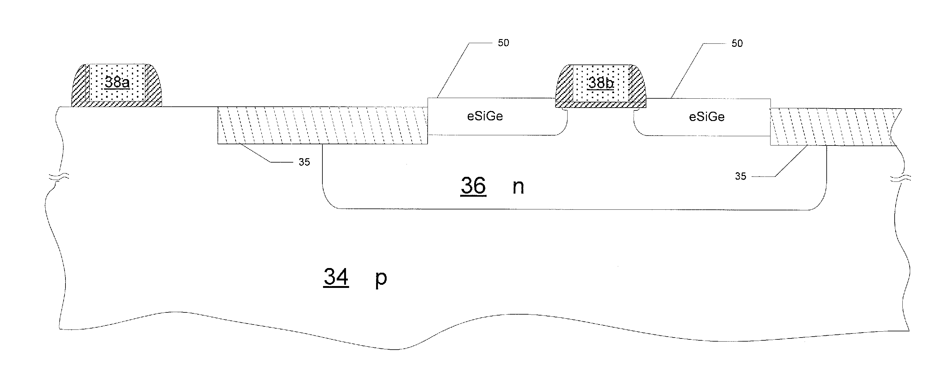
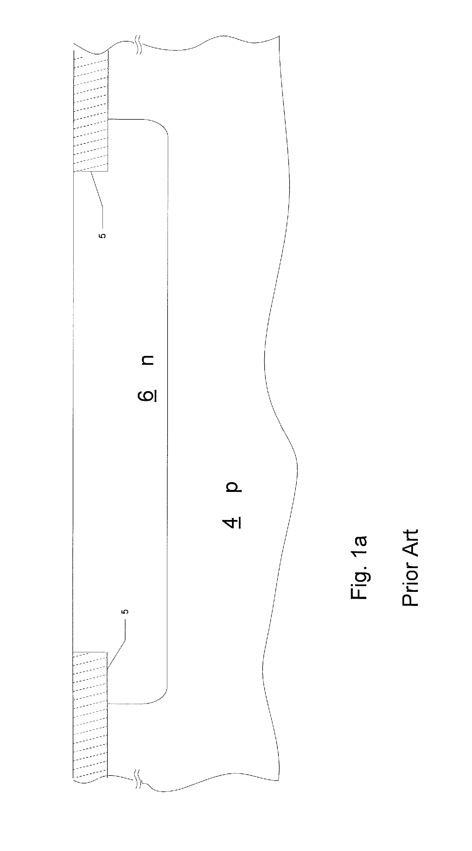
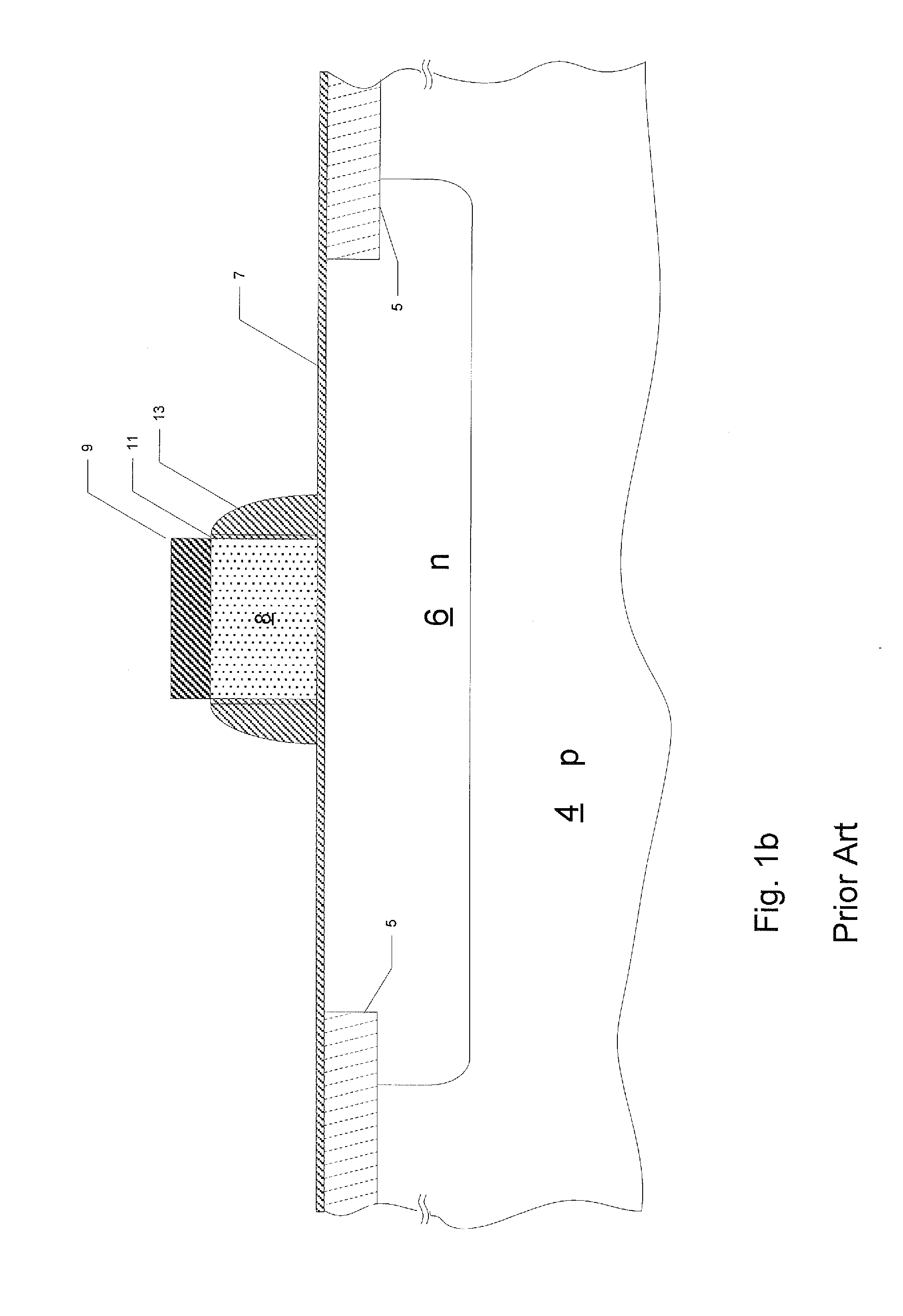
[0028]The present invention will be described in connection with its preferred embodiment, namely as implemented into a modern complementary metal-oxide-semiconductor (CMOS) fabrication process, as it is believed that this invention is especially beneficial when applied to such an application. However, it is contemplated that this invention can also provide important advantages and benefits when used in connection with other types of integrated circuits and technologies. Accordingly, it is to be understood that the following description is provided by way of example only, and is not intended to limit the true scope of this invention as claimed.

[0029]Many complex modern integrated circuits include circuitry for performing various functions. FIG. 2 illustrates the general layout of integrated circuit 10 which embodies a so-called “system on a chip” (SoC), which includes a wide range of functions to realize an overall system functionality. In this generalized example, logic circuitry 1...


PUM

PropertyMeasurementUnit
temperatureaaaaaaaaaa
pressureaaaaaaaaaa
poweraaaaaaaaaa

Abstract

A method of etching recesses into silicon prior to formation of embedded silicon alloy source / drain regions. The recess etch includes a plasma etch component, using an etch chemistry of a primary fluorine-based or chlorine-based etchant, in combination with a similar concentration of hydrogen bromide. The concentration of both the primary etchant and the hydrogen bromide is relatively low; a diluent of an inert gas or oxygen is added to the reactive species. Loading effects on the undercut of the recess etch are greatly reduced, resulting in reduced transistor performance variation.

Description

CROSS-REFERENCE TO RELATED APPLICATIONS[0001]Not applicable.STATEMENT REGARDING FEDERALLY SPONSORED RESEARCH OR DEVELOPMENT[0002]Not applicable.BACKGROUND OF THE INVENTION[0003]This invention is in the field of semiconductor integrated circuits. Embodiments of this invention are directed to uniformity of recess etch processes in connection with forming embedded silicon alloy structures.[0004]Recent advances in semiconductor technology as applied to integrated circuits include the use of “strain engineering” (or, alternatively, “stress engineering”) in the manufacture of semiconductor device structures. It has been discovered that the tuning of strain in the crystal lattice of metal-oxide-semiconductor (MOS) transistor channel regions can enhance carrier mobility in those regions. As is fundamental in MOS device technology, the source / drain current (i.e., drive) of an MOS transistor in both the triode and saturation regions is proportional to carrier mobility in the channel region. I...

Claims


Application Information

Patent Timeline
Patent Type & Authority Applications(United States)
IPC IPC(8): H01L21/336H01L21/3065
CPCH01L21/3065H01L21/823807H01L29/7848H01L29/66628H01L29/66636H01L21/823814
Inventor FARBER, DAVID GERALDLII, TOM
Owner TEXAS INSTR INC
Why Eureka
Try Eureka