Method for manufacturing semiconductor device

a manufacturing method and semiconductor technology, applied in semiconductor devices, capacitors, electrical devices, etc., can solve the problems of reducing the area on which a capacitor is formed, difficult to ensure the capacity required for a memory device, and the prospect of improving the features of a capacitor on the basis of these technical developments, etc., to achieve high reliability and high yield rate

Inactive Publication Date: 2012-03-15
PS4 LUXCO SARL
View PDF3 Cites 37 Cited by
  • Summary
  • Abstract
  • Description
  • Claims
  • Application Information

AI Technical Summary

Benefits of technology

[0013]The inventors found that a capacitor having a dielectric film, whose primary constituent is zirconium oxide of, for example, a ZAZ structure may prevent the increase in leakage current in spite of a heat treatment during the formation of an upper electrode and a hydrogen annealing for decreasing the interface state of transistors, if the capacitor is formed by forming a dielectric film comprising zirconium oxide in a microcrystal state as a primary constituent, forming a first protective film having titanium oxide as a primary constituent under a condition devoid of the secondary growth of crystal grains, and then forming an upper electrode. As described herein, the secondary growth of crystal grains means the rearrangement of constituent atoms by, for example, a heat treatment after film formation, and the change into larger crystal grains by the reformation of grain boundary.
[0026]According to the invention, the structure of a protective film inserted into the interface between the titanium nitride electrode and the dielectric film comprising zirconium oxide as a primary constituent can prohibit damages to the dielectric film caused by heat treatment during the formation of the upper electrode or by annealing for decreasing the interface state of transistors. As a result, restrictions, such as an upper limit in process temperature, imposed on a manufacturing process can be alleviated, and the characteristic of transistors can thus be compatible with that of capacitors. Accordingly, high reliability and a high yield rate can be accomplished for a device.

Problems solved by technology

As a result, the area on which a capacitor is formed decreases, and it is thus difficult to ensure the capacity required for a memory device.
Therefore, the prospect of improving the features of a capacitor on the basis of these technical developments is bleak.
However, a dielectric film made of a single body of zirconium oxide cannot achieve a sufficient thermostability, and leakage current likely increases after heat treatment.
However, this heat treatment, which is performed after forming a dielectric film comprising zirconium oxide such as a ZAZ structure as a principal component, may cause leakage current of a capacitor.
This result may impose restrictions on the manufacturing process, and make it difficult to achieve a good characteristic of transistors by a sufficient hydrogen annealing.

Method used


Image

  • Method for manufacturing semiconductor device
  • Method for manufacturing semiconductor device
  • Method for manufacturing semiconductor device

Examples


experiment 1

(Experiment 1)

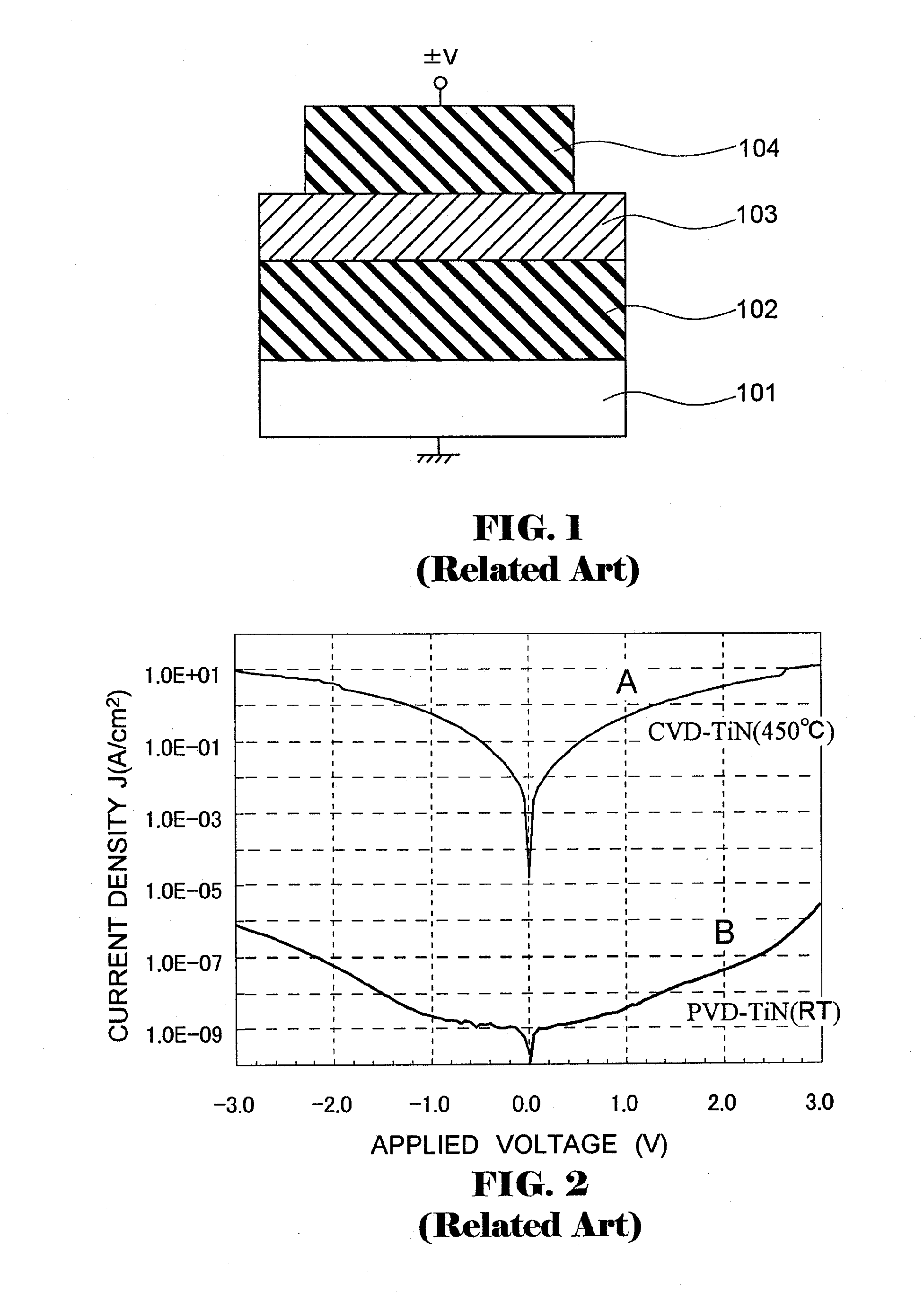
[0047]First, a capacitor having a single layer of a ZrO2 film (hereinafter referred to as “ZrO film”) has been evaluated.

[0048]FIG. 1 shows the structure of a flat capacitor including lower electrode 102 made of a titanium nitride film (TiN film), upper electrode 104 made of a TiN film in the same way, and dielectric film 103 made of a ZrO film sandwiched between the upper and lower electrodes.

[0049]Lower electrode 102 made of a TiN film has been formed using a chemical vapor deposition (CVD) method with reaction gases of titanium tetrachloride (TiCl4) and ammonia (NH3) in consideration of the application thereof to a three-dimensional structure. The deposition temperature was 450° C., and the thickness of the film was 10 nm. Hereinafter, a TiN film formed by a CVD method is referred to as a CVD-TiN film.

[0050]The ZrO film, which is to be dielectric film 103, has been formed using an atomic layer deposition (ALD) method with a reaction gas of ozone (O3) and a Zr precur...

experiment 2

(Experiment 2)

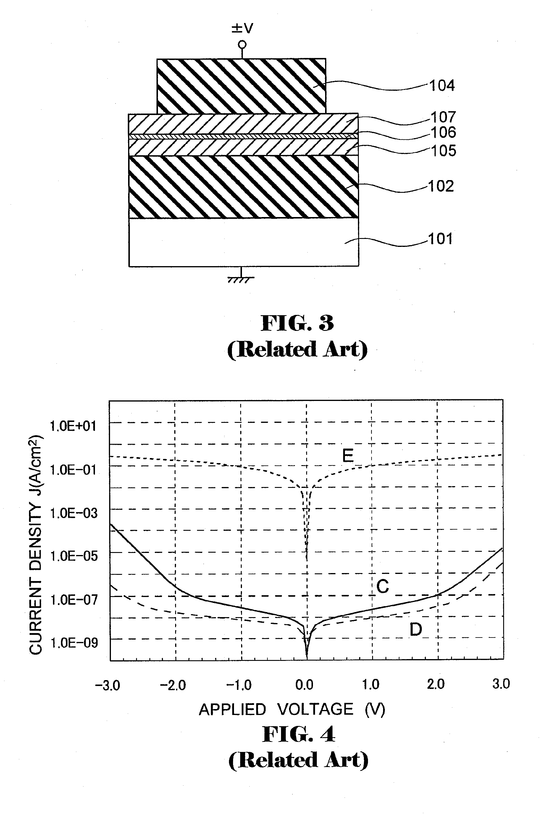
[0060]A capacitor with a ZAZ structure has been evaluated. The ZAZ structure is one of the dielectric film structures having zirconium oxide as a primary constituent, and one of the dielectric film structure within which aluminum oxide is included. A capacitor using a dielectric film of a ZAZ structure is referred to as a capacitor with a ZAZ structure.

[0061]FIG. 3 illustrates a flat capacitor including lower electrode 102 made of a CVD-TiN film, upper electrode 104 identically made of a CVD-TiN film, first dielectric film 105 made of a ZrO film formed on lower electrode 102, second dielectric film 106 made of an aluminum oxide film (hereinafter referred to as “AlO film”) formed on first dielectric film 105, and third dielectric film 107 made of a ZrO film formed on second dielectric film 106.

[0062]Lower electrode 102 made of a CVD-TiN film has been formed using a CVD method with reaction gases of titanium tetrachloride (TiCl4) and ammonia (NH3) in consideration of the...

experiment 3

(Experiment 3)

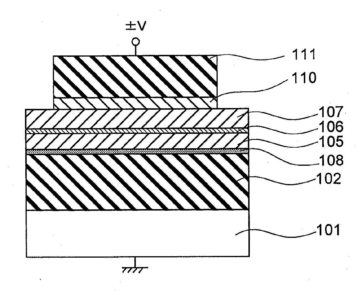
[0076]First, the inventors have been examined the effect of a titanium oxide film (hereinafter, a “TiO film”) as a protective film.

[0077]FIG. 5 shows a capacitor structure including, on semiconductor substrate 101, which is mono-crystalline silicon, lower electrode 102 made of a CVD-TiN film, dielectric film 103 made of a polycrystalline ZrO film, first protective film 110 made of a TiO film, and upper electrode 111 made of a CVD-TiN film. The capacitor structure in this experiment is not three-dimensional semiconductor memory device as explained above, and is constructed as a flat capacitor to achieve an easily manufacturable structure for evaluating its characteristics. For the purpose of comparison with Experiment 1, the dielectric film does not have a ZAZ structure, but a single film of a ZrO film.

[0078]As in Experiment 1, lower electrode 102 made of a CVD-TiN film is formed on semiconductor substrate 101 with a thickness of 10 nm, and a ZrO film is then formed for...


PUM

PropertyMeasurementUnit
forming temperatureaaaaaaaaaa
thicknessaaaaaaaaaa
thicknessaaaaaaaaaa

Abstract

A method for manufacturing a semiconductor device includes at least forming a lower electrode comprising titanium nitride on a semiconductor substrate, forming a dielectric film comprising zirconium oxide as a primary constituent on the lower electrode, forming a first protective film comprising a titanium compound on the dielectric film, and forming an upper electrode comprising titanium nitride on the first protective film. The method can include a step of forming a second protective film on the lower electrode before the step of forming the dielectric film on the lower electrode.

Description

BACKGROUND OF THE INVENTION[0001]1. Field of Invention[0002]The present invention relates to a semiconductor device and a method of manufacturing the same, and, in particular, to dynamic random access memory (DRAM) having a capacitor with properties of low leakage current and high permittivity.[0003]2. Description of Related Arts[0004]DRAM has been used for a semiconductor memory operable at a high speed in a computer or other electronic devices. DRAM has a memory cell array and a peripheral circuit for operating the array. The memory cell array has a plurality of units arranged in a matrix, and each unit comprises one switching transistor and one capacitor.[0005]As in other semiconductor devices, DRAM has developed with miniaturization of each cell to satisfy a demand for high-integration. As a result, the area on which a capacitor is formed decreases, and it is thus difficult to ensure the capacity required for a memory device. To solve this problem, a three-dimensional structure ...

Claims


Application Information

Patent Timeline
Patent Type & Authority Applications(United States)
IPC IPC(8): H01L21/02
CPCH01L21/02178H01L21/02189H01L21/022H01L21/0228H01L21/02304H01L21/02362H01L28/60H01L27/10814H01L27/10852H01L27/10894H01L28/40H01L28/75H01L28/91H01L27/0207H10B12/315H10B12/09H10B12/033
Inventor HIROTA, TOSHIYUKIKIYOMURA, TAKAKAZU
Owner PS4 LUXCO SARL
Why Eureka
Try Eureka