Plasma processing apparatus and plasma processing method

a processing apparatus and plasma technology, applied in the direction of plasma technique, electric discharge tube, decorative arts, etc., can solve the problems of difficult to have a sufficiently large area of the facing electrode, the plasma process cannot be performed stably, and the microwave becomes smaller, so as to suppress the oscillation of the plasma potential, suppress the sputtering, and the effect of large area

Active Publication Date: 2012-03-22
TOKYO ELECTRON LTD
View PDF7 Cites 25 Cited by
  • Summary
  • Abstract
  • Description
  • Claims
  • Application Information

AI Technical Summary

Benefits of technology

[0021]The plasma processing apparatus in accordance with the present disclosure may include the extended protrusion protruding from the processing chamber or the contact support toward the plasma generation space with the gap with respect to the dielectric plate. The extended protrusion may serve as a part of the second electrode facing the first electrode via the plasma generation space therebetween. Thus, the second electrode can have a sufficiently large area and oscillation of a plasma potential can be suppressed. Further, by increasing the second electr...

Problems solved by technology

If the path of the high frequency current is not formed stably, an oscillation amplitude of a plasma potential (Vp) generated within the processing chamber becomes large, and, thus, the plasma process cannot be performed stably.
Further, if the oscillation amplitude of the plasma potential is large, particularly when a process is performed at a low pressure of several tens Pa or less, a surface of the facing electrode typically made of aluminum may be sputtered by the plasma, resulting in contamination...

Method used


Image

  • Plasma processing apparatus and plasma processing method
  • Plasma processing apparatus and plasma processing method
  • Plasma processing apparatus and plasma processing method

Examples


first embodiment

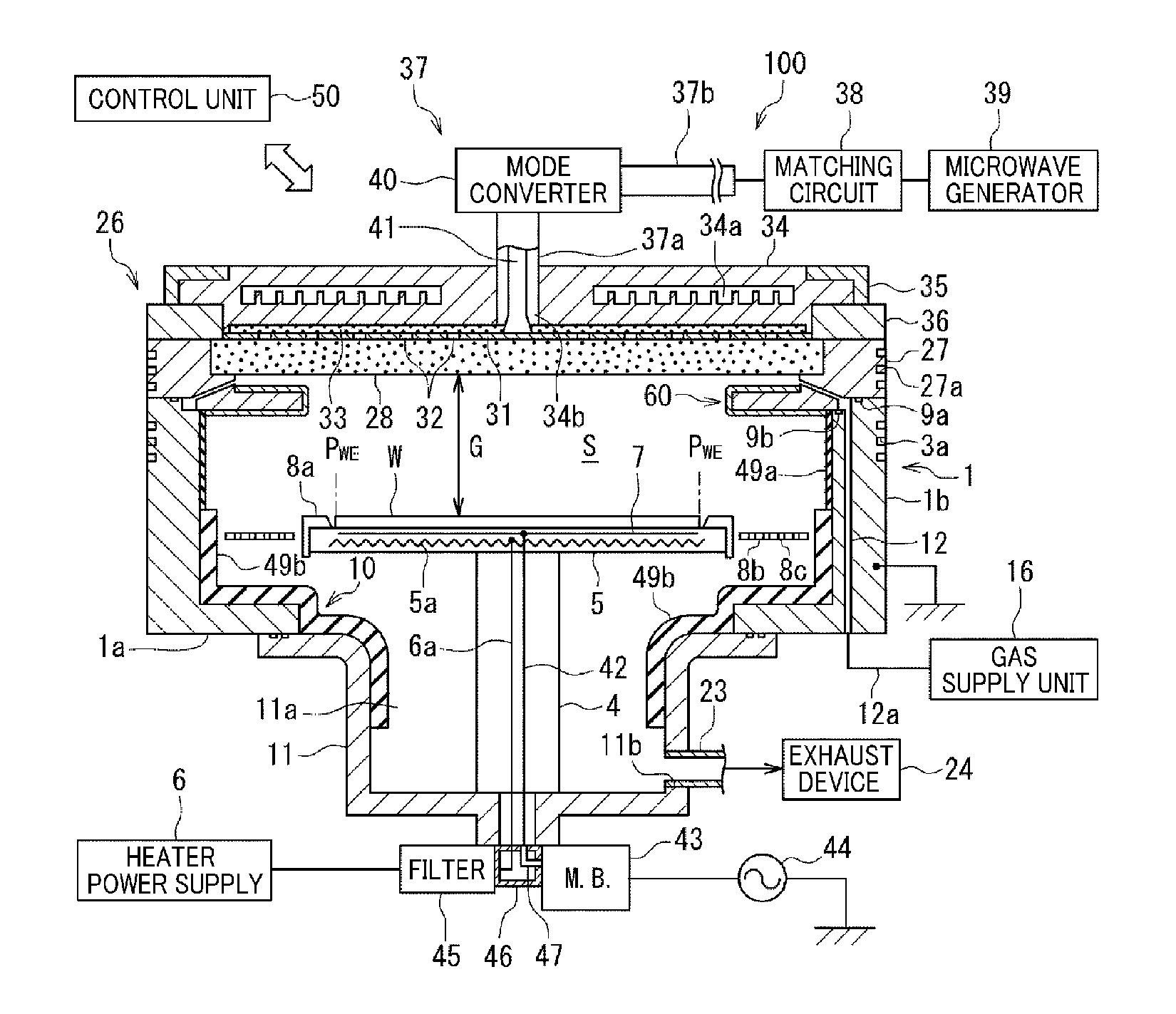
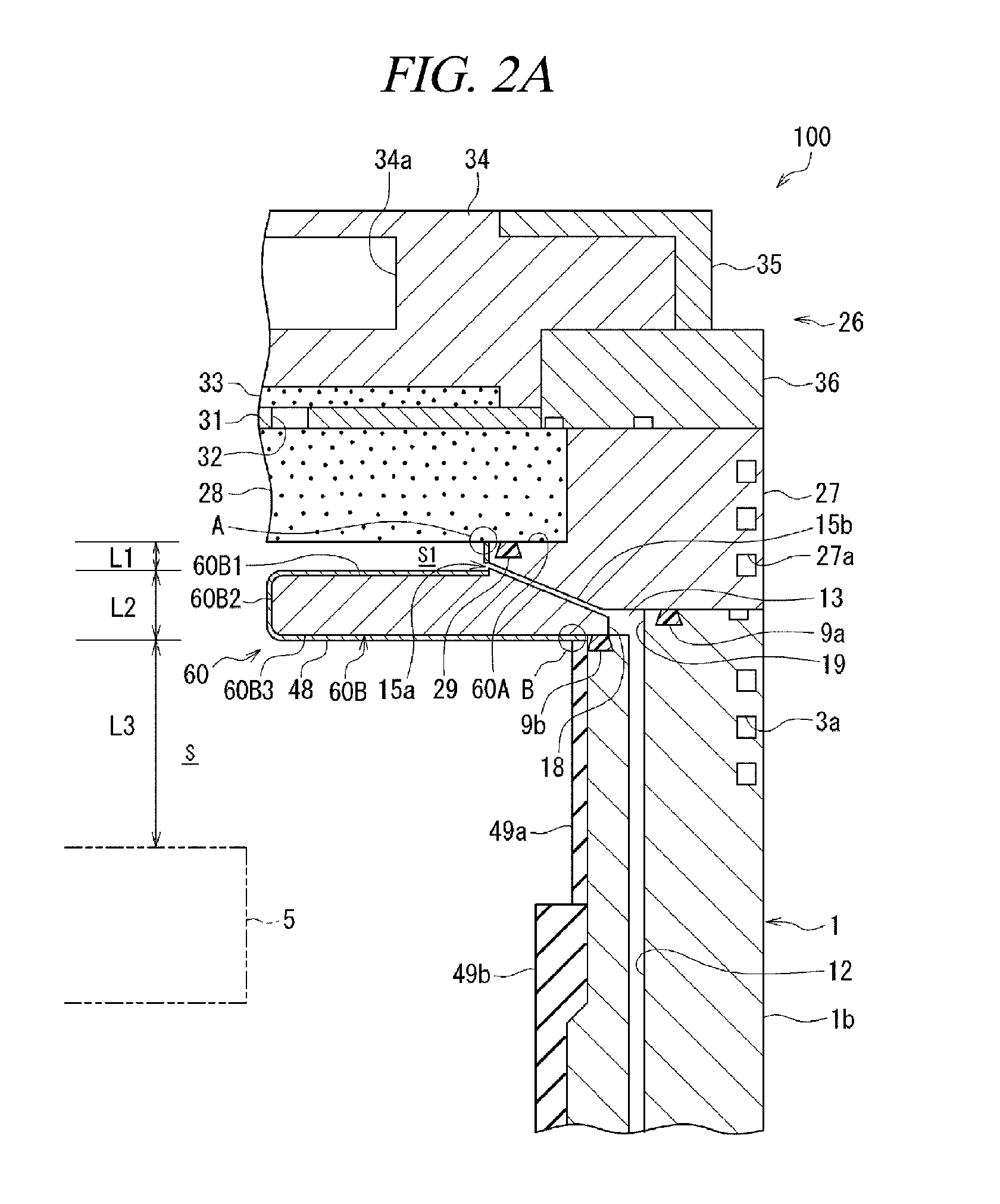
[0047]FIG. 1 is a schematic cross sectional view showing a configuration of a plasma processing apparatus 100 in accordance with a first embodiment of the present disclosure. FIG. 2A is a cross sectional view showing enlarged main parts of FIG. 1. FIG. 2B is a perspective view showing an external appearance of a cover as a component of the plasma processing apparatus 100. FIG. 3A shows a planar antenna of the plasma processing apparatus 100 of FIG. 1.

[0048]The plasma processing apparatus 100 may be configured as a RLSA microwave plasma processing apparatus capable of generating microwave excitation plasma having a high density and a low electron temperature within the processing chamber by introducing a microwave into a processing chamber through a planar antenna having multiple slot holes, particularly a RLSA (Radial Line Slot Antenna). In the plasma processing apparatus 100, a process can be performed by plasma having a plasma density in a range of from about 1×10¹⁰ / cm3 to about 5...

second embodiment

[0099]Hereinafter, a plasma processing apparatus in accordance with a second embodiment of the present disclosure will be explained with reference to FIG. 5. A plasma processing apparatus 101 in accordance with the second embodiment is the same, except its features, as the plasma processing apparatus 100 in accordance with the first embodiment. Therefore, explanation (FIGS. 1, 3A and 4) of the whole configuration will be omitted. Some components illustrated in FIG. 5 which are the same as the components illustrated in FIG. 2A will be assigned same reference numerals and explanation thereof will be omitted.

[0100]In the plasma processing apparatus 101 in accordance with the present embodiment, at an inner peripheral surface of a cover member 27, a protrusion 61 may constitute a part of the cover member 27. Since the cover member 27 and the protrusion 61 are formed as a single body, thermal conductivity and electric conductivity can be secured. The protrusion 61 may include a contact s...

third embodiment

[0111]Hereinafter, a plasma processing apparatus in accordance with a third embodiment of the present disclosure will be explained with reference to FIG. 6. A plasma processing apparatus 102 in accordance with the third embodiment is the same, except its features, as the plasma processing apparatus 100 in accordance with the first embodiment. Therefore, explanation (FIGS. 1, 3A and 4) of the whole configuration will be omitted. Some components illustrated in FIG. 6 which are the same as the components illustrated in FIG. 2A will be assigned same reference numerals and explanation thereof will be omitted.

[0112]In the plasma processing apparatuses in accordance with the first and second embodiments, extended protrusions 60B and 61B may be respectively formed at protrusions 60 and 61 of a cover member 27 as the facing electrode. However, in the plasma processing apparatus 102 in accordance with the present embodiment, an extended protrusion 62 protruding inwards may be formed at an upp...


PUM

PropertyMeasurementUnit
Lengthaaaaaaaaaa
Lengthaaaaaaaaaa
Pressureaaaaaaaaaa

Abstract

There is provided a plasma processing apparatus capable of stably generating plasma by suppressing oscillation of a plasma potential, and capable of preventing contamination caused by sputtering a facing electrode made of metal. A high frequency bias power is applied to an electrode within a mounting table for mounting a target object thereon. An extended protrusion 60 is formed at an inner peripheral surface of a cover member 27. The extended protrusion 60 is formed toward a plasma generation space S and serves as a facing electrode facing an electrode 7 within a mounting table 5 with the plasma generation space S therebetween. A ratio of a surface area of the facing electrode with respect to that of an electrode for bias (facing electrode surface area/bias electrode area) is in a range of from about 1 to about 5.

Description

CROSS-REFERENCE TO RELATED APPLICATION[0001]This application claims the benefit of Japanese Patent Application Nos. 2010-207772 and 2011-163750 filed on Sep. 16, 2010 and Jul. 26, 2011, respectively, the entire disclosures of which are incorporated herein by reference.FIELD OF THE INVENTION[0002]The present disclosure relates to a plasma processing apparatus and a plasma processing method for performing a plasma process on a target object such as a semiconductor wafer.BACKGROUND OF THE INVENTION[0003]In a manufacturing process of a semiconductor device, various processes such as an etching process, an ashing process and a film forming process have been performed on a semiconductor wafer as a target object. In these processes, there has been used a plasma processing apparatus configured to perform a plasma process on the semiconductor wafer in a processing chamber capable of maintaining a vacuum atmosphere.[0004]Recently, a semiconductor wafer has become larger and a device has becom...

Claims


Application Information

Patent Timeline
IPC IPC(8): H01L21/3065H01L21/306
CPCH01J37/32192H01J37/32541
Inventor MONDEN, TAICHIKITAGAWA, JUNICHIYAMASHITA, JUNNAKAMURA, HIDEO
Owner TOKYO ELECTRON LTD
Why Eureka
Try Eureka