Resist underlayer film forming composition containing silicon having sulfide bond

a technology of resisting and underlayer film, applied in the direction of photomechanical equipment, instruments, transportation and packaging, etc., can solve the problem of large influence of active ray reflection on semiconductor substrates

Active Publication Date: 2012-03-22
NISSAN CHEM IND LTD
View PDF3 Cites 22 Cited by
  • Summary
  • Abstract
  • Description
  • Claims
  • Application Information

AI Technical Summary

Benefits of technology

[0016]The present invention relates to, according to a first aspect, a resist underlayer film forming composition for lithography containing, as a silicon atom-containing compound, at least one of compound selected from a group consisting of a hydrolyzable

Problems solved by technology

Following such a tendency, the influence of reflection of an act

Method used


Image

  • Resist underlayer film forming composition containing silicon having sulfide bond
  • Resist underlayer film forming composition containing silicon having sulfide bond
  • Resist underlayer film forming composition containing silicon having sulfide bond

Examples


synthesis example 1

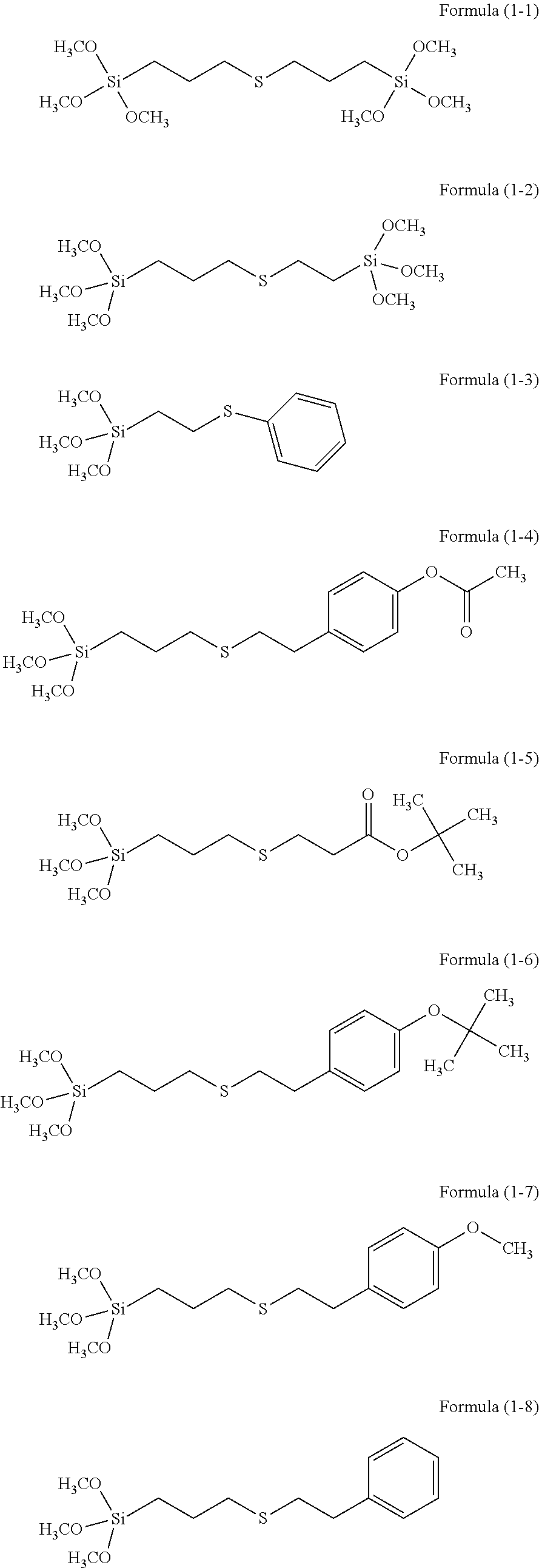
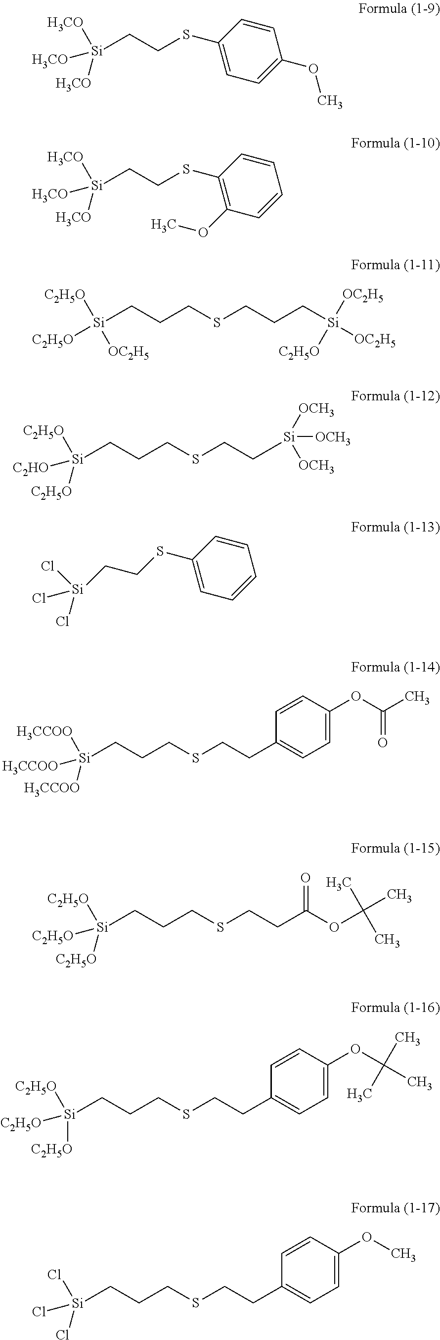
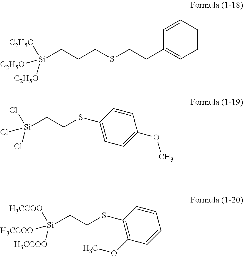
[0215]0.18 g of a compound of Formula (1-1), 13.54 g of tetraethoxysilane, 1.98 g of phenyltrimethoxysilane, 4.37 g of methyltriethoxysilane, and 30.11 g of acetone were charged into a 100 mL flask to be dissolved and the resultant reaction mixture was warmed while being stirred with a magnetic stirrer to be refluxed. Next, to the reaction mixture, an aqueous solution in which 0.01 g of hydrochloric acid was dissolved in 6.60 g of ion-exchanged water was added. The resultant reaction mixture was subjected to the reaction for 240 minutes and the resultant reaction solution was cooled down to room temperature. Then, to the reaction solution, 21.00 g of propylene glycol monomethyl ether acetate was added and ethanol that was a reaction by-product, water, and hydrochloric acid were distilled off under reduced pressure to obtain a solution of a hydrolysis-condensation product (polyorganosiloxane). The obtained polymer had a weight average molecular weight Mw measured by GPC in terms of p...

synthesis example 2

[0216]1.75 g of a compound of Formula (1-1), 13.54 g of tetraethoxysilane, 1.98 g of phenyltrimethoxysilane, 3.58 g of methyltriethoxysilane, and 31.32 g of acetone were charged into a 100 mL flask to be dissolved and the resultant reaction mixture was warmed while being stirred with a magnetic stirrer to be refluxed. Next, to the reaction mixture, an aqueous solution in which 0.01 g of hydrochloric acid was dissolved in 6.85 g of ion-exchanged water was added. The resultant reaction mixture was subjected to the reaction for 240 minutes and the resultant reaction solution was cooled down to room temperature. Then, to the reaction solution, 21.00 g of propylene glycol monomethyl ether acetate was added and ethanol that was a reaction by-product, water, and hydrochloric acid were distilled off under reduced pressure to obtain a solution of a hydrolysis-condensation product (polyorganosiloxane). The obtained polymer had a weight average molecular weight Mw measured by GPC in terms of p...

synthesis example 3

[0217]0.144 g of a compound of Formula (1-3), 15.05 g of tetraethoxysilane, 0.99 g of phenyltrimethoxysilane, 5.94 g of methyltriethoxysilane, and 33.19 g of acetone were charged into a 100 mL flask to be dissolved and the resultant reaction mixture was warmed while being stirred with a magnetic stirrer to be refluxed. Next, to the reaction mixture, an aqueous solution in which 0.01 g of hydrochloric acid was dissolved in 7.30 g of ion-exchanged water was added. The resultant reaction mixture was subjected to the reaction for 240 minutes and the resultant reaction solution was cooled down to room temperature. Then, to the reaction solution, 22.00 g of propylene glycol monomethyl ether acetate was added and ethanol that was a reaction by-product, water, and hydrochloric acid were distilled off under reduced pressure to obtain a solution of a hydrolysis-condensation product (polyorganosiloxane). The obtained polymer had a weight average molecular weight Mw measured by GPC in terms of ...


PUM

PropertyMeasurementUnit
Percent by moleaaaaaaaaaa
Angleaaaaaaaaaa

Abstract

There is provided a resist underlayer film forming composition for lithography for forming a resist underlayer film capable of being used as a hard mask; and a forming method of a resist pattern using the underlayer film forming composition for lithography. A resist underlayer film forming composition for lithography comprising: as a silicon atom-containing compound, a hydrolyzable organosilane containing a sulfur atom-containing group, a hydrolysis product thereof, or a hydrolysis-condensation product thereof, wherein in the whole silicon atom-containing compound, the ratio of a sulfur atom to a silicon atom is less than 5% by mole. The hydrolyzable organosilane is preferably a compound of Formula (1): [R1aSi(R2)3-a]bR3 wherein R3 has a partial structure of Formula (2): R4—S—R5.

Description

TECHNICAL FIELD[0001]The present invention relates to a composition for forming an underlayer film between a substrate and a resist (for example, a photoresist and an electron beam resist) that are used in the production of semiconductor devices. More specifically, the present invention relates to a resist underlayer film forming composition for lithography for forming an underlayer film used for an underlayer of a photoresist in a lithography process of the production of semiconductor devices. In addition, the present invention relates to a forming method of a resist pattern using the underlayer film forming composition.BACKGROUND ART[0002]Conventionally, in the production of semiconductor devices, microfabrication by lithography using a photoresist has been performed. The microfabrication is a processing method for forming fine convexo-concave shapes corresponding to the following pattern on the surface of a substrate by: forming a thin film of a photoresist on a semiconductor sub...

Claims


Application Information

Patent Timeline
IPC IPC(8): H01L21/312C07F7/18B32B9/00C08K5/548
CPCG03F7/0752G03F7/11G03F7/091Y10T428/31663
Inventor KANNO, YUTANAKAJIMA, MAKOTOSHIBAYAMA, WATARU
Owner NISSAN CHEM IND LTD
Why Eureka
Try Eureka