Method for manufacturing silicon thin-film solar cells

a technology of solar cells and silicon thin films, applied in the field of manufacturing silicon thin films solar cells, can solve the problems of lower photoelectric conversion efficiency of monocrystalline or polycrystalline silicon solar cells, and the drawback of photodegradation

Inactive Publication Date: 2012-04-26
NAT CENT UNIV
View PDF5 Cites 11 Cited by
  • Summary
  • Abstract
  • Description
  • Claims
  • Application Information

AI Technical Summary

Benefits of technology

[0031]In the following examples, a p-type amorphous silicon layer, amorphous / nanocrystalline silicon layers, and an n-type amorphous / nano-microcrystalline silicon layer were formed by electron cyclotron resonance chemical vapor deposition (ECRCVD). Herein, the amorphous / nanocrystalline silicon layers were formed in the condition as follows: the substrate temperature of about 60° C. to 350° C., the microwave power of about 500 W to 1500 W, the deposition pressure of about 1 mTorr to 30 mTorr, the He flow of about 10 sccm to 30 sccm, the SiH4 flow of about 5 sccm to 30 sccm, and the H2 flow of about 0 sccm to 300 sccm (i.e. H2 / SiH4+H2 of about 0% to 98%). Additionally, in the following examples, the variation of the amorphous / nanocrystalline silicon layers in average grain sizes can be achieved by altering (1) the ratio of silicon source to hydrogen, (2) the microwave power, (3) the ratio of silicon source to hydrogen and deposition temperature under CF4 flow of about 2 sccm to 5 sccm, (4) microwave power and deposition temperature, or (5) microwave power and deposition pressure, such that an intrinsic layer with graded bandgaps can be formed. Moreover, the following examples used an alpha-step profilometer (veeco dektak 6M) to measure the thickness of each thin film and a Raman spectrometer (Raman Imaging Microscope System 1000, available from RENISHAW Co.) to qualitatively analyze the crystal quality and atomic bonding of each silicon film. A board peak can be found at about 480 cm−1 for amorphous silicon phase, while a sharp peak would be found at about 510-520 cm−1 for nanocrystalline or microcrystalline phase. Furthermore, the following examples used an X-ray diffractometer (D & DISCOVER X-ray Diffractometer, available from BRUKER Co.) with a Cu Kα (1.54056 Å) to observe the crystal and to determine its grain size by Scherrer's equation.

Problems solved by technology

Among them, amorphous silicon solar cells can be fabricated in lower cost, but exhibit lower photoelectric conversion efficiency than monocrystalline or polycrystalline silicon solar cells and have the drawback of photodegradation.
Although broadband absorption can be achieved by stacking PIN junction units of different bandgaps, the choice of material used in the tandem solar cells is limited in consideration of current matching, and the method for fabricating the tandem solar cells is more complex.
Additionally, the manufacture of the intermediate layer for the enhancement of the photoelectric conversion efficiency is difficult and causes an increase in manufacturing cost.

Method used


Image

  • Method for manufacturing silicon thin-film solar cells
  • Method for manufacturing silicon thin-film solar cells
  • Method for manufacturing silicon thin-film solar cells

Examples


example 1

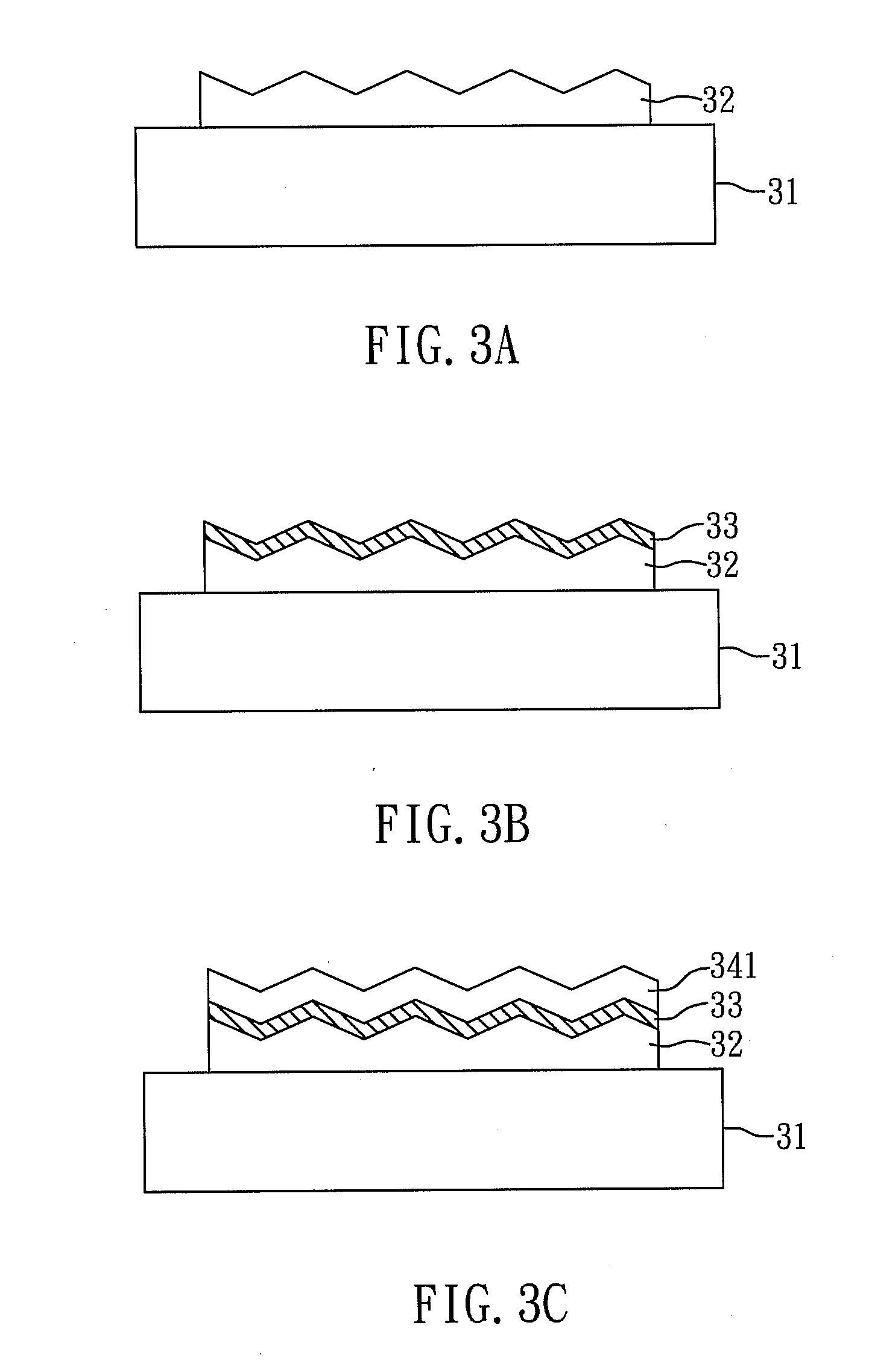
[0032]FIGS. 3A to 3G show cross-sectional views for illustrating the method for manufacturing a silicon thin-film solar cell according to the present example.

[0033]As shown in FIG. 3A, a substrate 31 was first provided and a first electrode 32 was formed on the substrate 31. In the present example, a transparent glass substrate was utilized as the substrate 31, and transparent ITO material was coated on the substrate 31 by sputtering to form a first transparent conductive oxide layer as the first electrode 32. Accordingly, incident light can pass through the substrate 31 and the first electrode 32.

[0034]Next, the present example utilized electron cyclotron resonance chemical vapor deposition (ECRCVD) to grow the subsequent silicon thin films.

[0035]As shown in FIG. 3B, a first doped semiconductor layer 33 was formed on the first electrode 32 by ECRCVD. In detail, a p-type amorphous silicon layer was grown as the first doped semiconductor layer 33 in the condition as follows: the subs...

example 2

[0039]FIGS. 4A to 4E show cross-sectional views for illustrating the method for manufacturing a silicon thin-film solar cell according to the present example.

[0040]As shown in FIG. 4A, a substrate 31 was first provided and a first electrode 32 was formed on the substrate 31. In the present example, a stainless steel substrate was utilized as the substrate 31, and Ag (i.e. a metal layer 321) and ZnO (i.e. a first transparent oxide layer 322) were coated on the substrate 31 by sputtering to form the first electrode 32.

[0041]Next, the present example utilized electron cyclotron resonance chemical vapor deposition (ECRCVD) to grow the subsequent silicon thin films.

[0042]As shown in FIG. 4B, a first doped semiconductor layer 33 was formed on the first electrode 32 by ECRCVD. In detail, an n-type amorphous / nano-microcrystalline silicon layer of 300 Å in thickness was grown as the first doped semiconductor layer 33 in the condition as follows: the substrate temperature of about 250° C., th...

example 3

[0046]FIGS. 5A to 5C show cross-sectional views for illustrating the method for manufacturing a silicon thin-film solar cell according to the present example.

[0047]First, a structure as shown in FIG. 5A was fabricated by the process illustrated in FIGS. 3A to 3B.

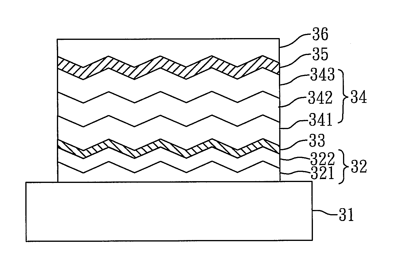
[0048]Subsequently, as shown in FIG. 5B, the present example utilized ECRCVD and modified the microwave power and the substrate temperature to form an intrinsic layer 34 with bandgaps varied in an approximate V-shaped trend from the side of the p-type amorphous silicon layer on the first doped semiconductor layer 33. In detail, a first amorphous / nanocrystalline silicon layer 341, a second amorphous / nanocrystalline silicon layer 342, a third amorphous / nanocrystalline silicon layer 343 and a fourth amorphous / nanocrystalline silicon layer 344 were formed on the p-type amorphous silicon layer in sequence by modifying the substrate temperature and the microwave power in a constant condition as follows: the deposition pressure of ...


PUM

PropertyMeasurementUnit
temperatureaaaaaaaaaa

Abstract

The present invention relates to a method for manufacturing silicon thin-film solar cells, including: providing a substrate; forming a first electrode on the substrate; forming a first doped semiconductor layer on the first electrode by chemical vapor deposition; forming an intrinsic layer on the first doped semiconductor layer by chemical vapor deposition, where the intrinsic layer includes a plurality of amorphous/nanocrystalline silicon layers, and the intrinsic layer has various energy bandgaps formed by varying average grain sizes of the amorphous/nanocrystalline silicon layers; forming a second doped semiconductor layer on the intrinsic layer by chemical vapor deposition, where one of the first doped semiconductor layer and the second doped semiconductor layer is a p-type amorphous silicon layer and the other is an n-type amorphous/nano-microcrystalline silicon layer; and forming a second electrode on the second doped semiconductor layer. Accordingly, the present invention can achieve broadband absorption in a single junction structure.

Description

CROSS REFERENCE TO RELATED APPLICATION[0001]This application claims the benefits of the Taiwan Patent Application Serial Number 100101245, filed on Jan. 13, 2011, the subject matter of which is incorporated herein by reference.BACKGROUND OF THE INVENTION[0002]1. Field of the Invention[0003]The present invention relates to a method for manufacturing silicon thin-film solar cells, more particularly, to a method for manufacturing silicon thin-film solar cells with graded bandgaps.[0004]2. Description of Related Art[0005]Due to the finite nature of conventional energy such as petroleum and coal, alternative forms of energy have been developed to replace the conventional energy. Among all the forms of alternative energy, solar energy is abundant and environmentally friendly, so research about solar cells has been vigorously pursued. The solar cell is a photovoltaic device to convert light into electricity, and the structurally simplest solar cell is a single junction solar cell. As shown...

Claims


Application Information

Patent Timeline
Patent Type & Authority Applications(United States)
IPC IPC(8): H01L31/18
CPCH01L31/0376H01L31/03845Y02E10/545Y02E10/548H01L31/1804H01L31/03685H01L31/03762H01L31/065H01L31/075Y02E10/547Y02P70/50
Inventor LI, TOMI T.CHANG, JENQ-YANGCHEN, SHENG-HUILEE, CHENG-CHUNG
Owner NAT CENT UNIV
Why Eureka
Try Eureka