Copper conductor film and manufacturing method thereof, conductive substrate and manufacturing method thereof, copper conductor wiring and manufacturing method thereof, and treatment solution

a manufacturing method and copper conductor technology, applied in the direction of resistive material coating, solid-state device coating, metallic material coating process, etc., can solve the problem of increasing the unit price of superfine printing dispersion slurry, the inability to print wiring having a line width not more than the particle diameter, and the inability to form fine wiring patterns. , to achieve the effect of not causing a fall in electric conductance, excellent conductivity and wiring pattern formation

Inactive Publication Date: 2012-05-24
HITACHI CHEM CO LTD
View PDF3 Cites 17 Cited by
  • Summary
  • Abstract
  • Description
  • Claims
  • Application Information

AI Technical Summary

Benefits of technology

[0077]According to the invention, it is possible to provide a copper conductor film that can be manufactured at a relatively low temperature, is excellent in conductivity and for wiring pattern formation, and does not cause a fall in electric conductance between circuits even when the wiring line width and the space between the wiring lines are narrow, a manufacturing method thereof, and patterned copper conductor wiring.
[0078]According to the invention, it is also possible to provide a manufacturing method of a conductive substrate that includes the step of treating a layer containing a copper oxide and the like by using a treatment solution which contains, in the single solution, a chemical agent capable of ionizing or complexing a copper oxide, and a reducing agent for reducing a copper ion or a copper complex to be made into metallic copper, thereby precipitating copper, and that can give a conductive layer low in resistance and restrain copper from precipitating in regions other than a desired region, and a conductive substrate yielded by the manufacturing method.
[0079]Furthermore, according to the invention, it is possible to provide a manufacturing method of a copper wiring substrate that includes

Problems solved by technology

Moreover, in conventional silver pastes, silver particles are in the form of flakes having from 1 to 100 μm in particle diameter; therefore, it is in principle impossible to print wiring having a line width not more than the particle diameter of the flake-form silver particles.
From these viewpoints, conventional paste is unsuitable for forming a fine wiring pattern.
However, when using nanoparticles of a noble metal such as gold or silver, the unit price for producing a superfine-printing dispersion slurry thereof also increases since the material itself is expensive.
This matter is a seriously large economic obstacle against the spread of the article as a versatile article into a wide range.
Furthermore, as the width of wiring lines a

Method used


Image

  • Copper conductor film and manufacturing method thereof, conductive substrate and manufacturing method thereof, copper conductor wiring and manufacturing method thereof, and treatment solution
  • Copper conductor film and manufacturing method thereof, conductive substrate and manufacturing method thereof, copper conductor wiring and manufacturing method thereof, and treatment solution
  • Copper conductor film and manufacturing method thereof, conductive substrate and manufacturing method thereof, copper conductor wiring and manufacturing method thereof, and treatment solution

Examples


example 1

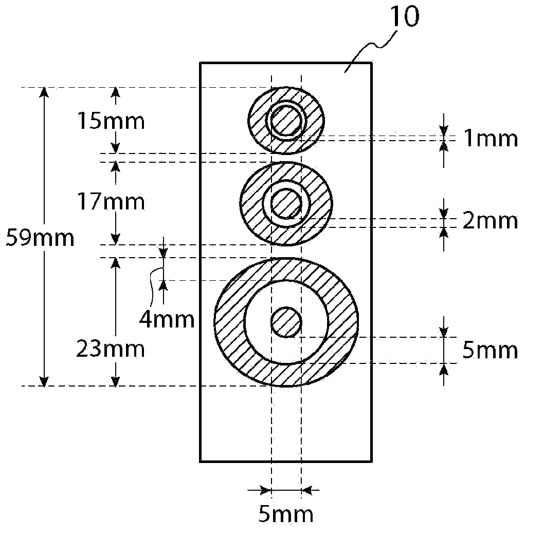
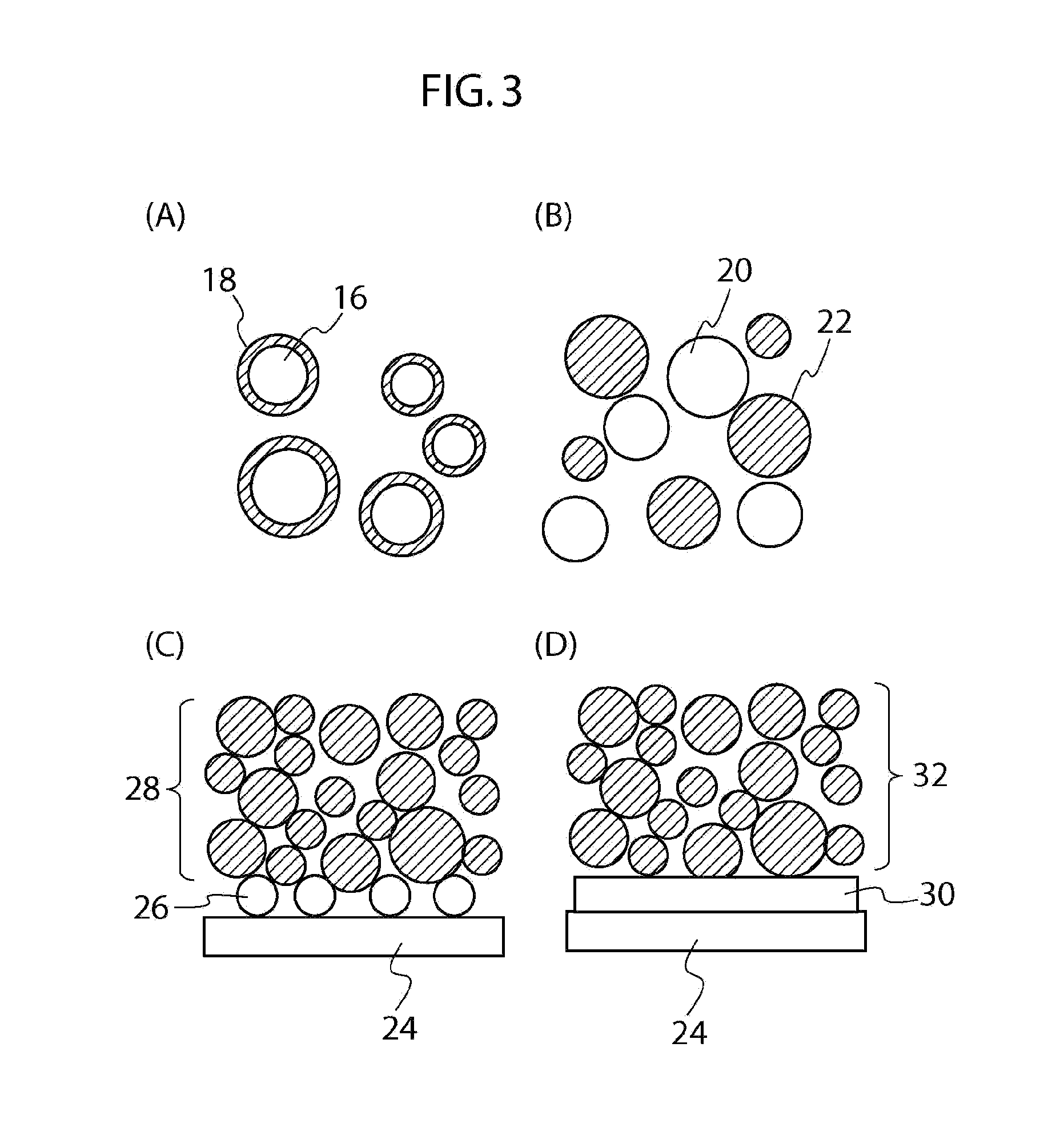
[0283]As a substrate on which copper nanoparticles were deposited, the following was used: a substrate having a copper nanoparticle deposited layer (copper based particle containing layer) yielded by painting a 5% by mass dispersion slurry of copper nanoparticles (trial product, manufactured by Fukuda Metal Foil & Powder Co., Ltd.), produced in a solution by a laser ablation process, in γ-butyrolactone onto a polyimide substrate (trade name: MCF-5000I, manufactured by Hitachi Chemical Co., Ltd.) having copper patterns in FIG. 4 by means of an applicator, and then repeating the drying of the resultant at 100° C. under a nitrogen atmosphere 3 times.

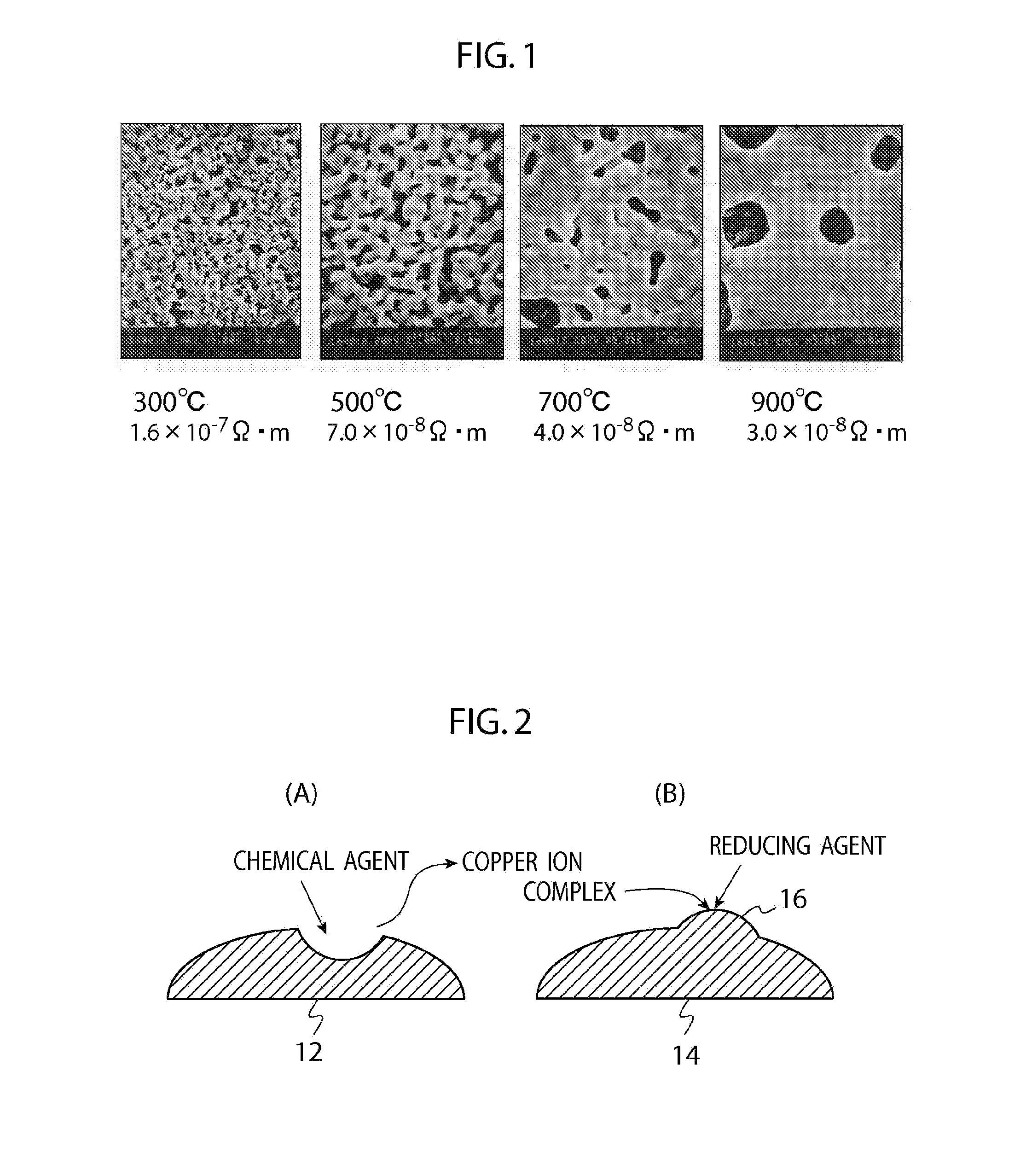
[0284]It is understood from Auger electron spectroscopy and STEM-EDX observation that the present particles had a core / shell structure wherein a copper oxide layer was present around metallic copper.

[0285]A solution prepared by weighing in accordance with column 1 in Table 1 was used as a treatment solution. The substrate having the copper ...

example 2

[0288]In accordance with the blend table (column 2 in Table 1), a substrate as used in Example 1, which had a deposit film of the copper nanoparticles, was prepared. The substrate was treated with a treatment solution for conversion to a conductor (treatment solution) neither containing 2,2′ bipyridyl nor EDTA in the same way as in Example 1. As a result, in the concentrically-circular copper patterns having gaps of 1 mm, 2 mm and 5 mm, respectively, resistances of 25 Ω, 28Ω and 238Ω were shown, respectively; thus, high electroconductivity was shown.

example 3

[0289]In accordance with the blend table (column 3 in Table 1), a substrate as used in Example 1, which had a deposit film of the copper nanoparticles, was prepared. The substrate was treated with a treatment solution for conversion to a conductor (treatment solution) using ethylenediamine instead of ammonia in the same way as in Example 1. As a result, in the concentrically-circular copper patterns having gaps of 1 mm, 2 mm and 5 mm, respectively, resistances of 9.8 MΩ, and 131Ω were shown, respectively; thus, electroconductivity was shown.


PUM

PropertyMeasurementUnit
Electrical conductoraaaaaaaaaa
Catalytic activityaaaaaaaaaa
Molar ratioaaaaaaaaaa

Abstract

Provided are a copper conductor film and manufacturing method thereof, and patterned copper conductor wiring, which have superior conductivity and wiring pattern formation, and with which there is no decrease in insulation between circuits, even at narrow wiring widths and narrow inter-wiring spacing. Disclosed are a copper conductor film and manufacturing method thereof in which a copper-based particle-containing layer, which contains both a metal having catalytic activity toward a reducing agent and copper oxide, is treated using a treatment solution that contains a reagent that ionizes or complexes copper oxide and a reducing agent that reduces copper ions or copper complex to form metallic copper in a single solution, and patterned copper conductor wiring that is obtained by patterning a copper-based particle-containing layer using printing and by said patterned particle-containing layer being treated by a treatment method using a solution that contains both a reagent that ionizes or complexes copper oxide and a reducing agent that reduces copper ions or copper complexes to form metallic copper in a single solution.

Description

1. TECHNICAL FIELD[0001]The present invention relates to a copper conductor film and a manufacturing method thereof, a conductive substrate and a manufacturing method thereof, copper conductor wiring and a manufacturing method thereof, and a treatment solution.2. BACKGROUND ART[0002]The formation of a wiring pattern by printing has been expected to be promising because of low energy, low costs, high throughput, on-demand production, and other superiorities. This purpose is achieved by following technique: an ink paste containing a metal element is used to form a pattern by printing, and then metallic conductivity is given to the printed wiring pattern.[0003]Hitherto, for this purpose, a paste has been used wherein silver or copper in a flake form is incorporated, together with an organic solvent, a curing agent, a catalyst and the like, into a binder of a thermoplastic resin or thermosetting resin. The using method of this paste is conducted by painting the paste onto a target objec...

Claims


Application Information

Patent Timeline
IPC IPC(8): H01B5/00C22B15/00C09K3/00B05D3/00B32B15/20C22C9/00B05D5/12
CPCC23C18/1601Y10T428/12014C23C18/1633C23C18/1635C23C18/1637C23C18/1824C23C18/1872C23C18/30C23C18/40H01L24/29H01L2924/01004H01L2924/01013H01L2924/01029H01L2924/01033H01L2924/01046H01L2924/01047H01L2924/0105H01L2924/0106H01L2924/01078H01L2924/01079H01L2924/09701H01L2924/19043H05K3/105H05K3/1241H05K3/182H05K2203/0315H05K2203/0709H05K2203/1157H05K2203/125H01L2224/29H01L2224/2919H01L2924/01005H01L2924/01006H01L2924/01044H01L2924/01045H01L2924/0665C23C18/1603Y10T428/12903H01L2924/00013H01L2224/29347H01L2924/01019H01L2924/00H01L2924/00014H01L2224/29099H01L2224/29199H01L2224/29299H01L2224/2929H01L2224/8384H01L2224/29294H01L2924/203H01L2924/12042H01L2924/0002
Inventor NAKAKO, HIDEOYAMAMOTO, KAZUNORIKUMASHIRO, YASUSHIMACHII, YOUICHIYOKOZAWA, SHUNYAEJIRI, YOSHINORIMASUDA, KATSUYUKI
Owner HITACHI CHEM CO LTD
Why Eureka
Try Eureka