Sos substrate having low defect density in the vicinity of interface

Inactive Publication Date: 2012-05-24
SHIN ETSU CHEM IND CO LTD
View PDF2 Cites 7 Cited by
  • Summary
  • Abstract
  • Description
  • Claims
  • Application Information

AI Technical Summary

Benefits of technology

[0011]In view of the current circumstances, an object of the invention is to solve a problem that a defect density increases due to lattice constant

Problems solved by technology

However, use of the heteroepitaxial SOS substrate is limited to small individual parts such as a switch at present since a defect density is high.
However, even if the double solid phase growth method is used, the defect density is about 106 to 107 pieces/cm2 so that it is difficult to make a recent highly downscaled

Method used


Image

  • Sos substrate having low  defect density in the vicinity of interface
  • Sos substrate having low  defect density in the vicinity of interface
  • Sos substrate having low  defect density in the vicinity of interface

Examples


example 1

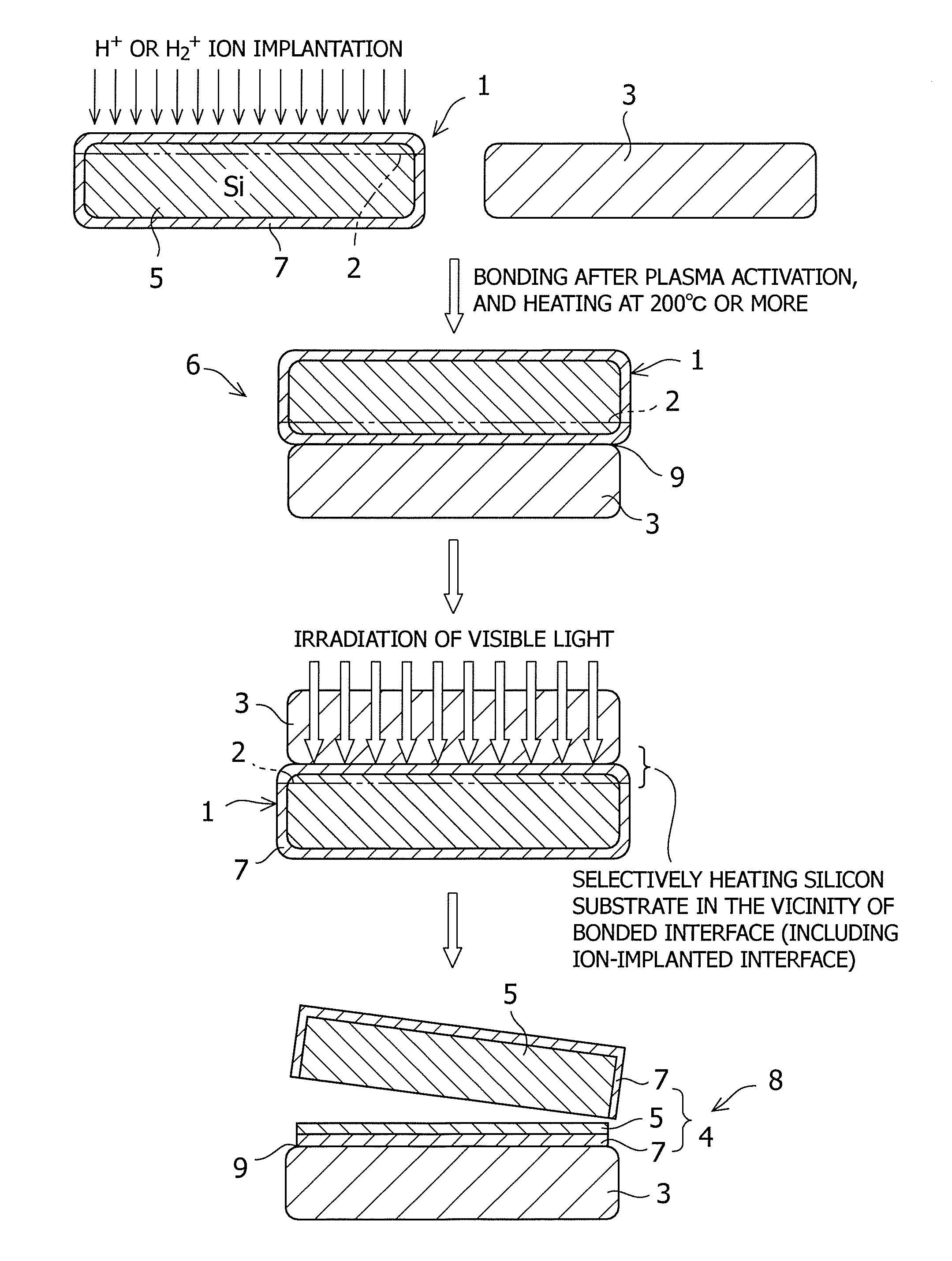
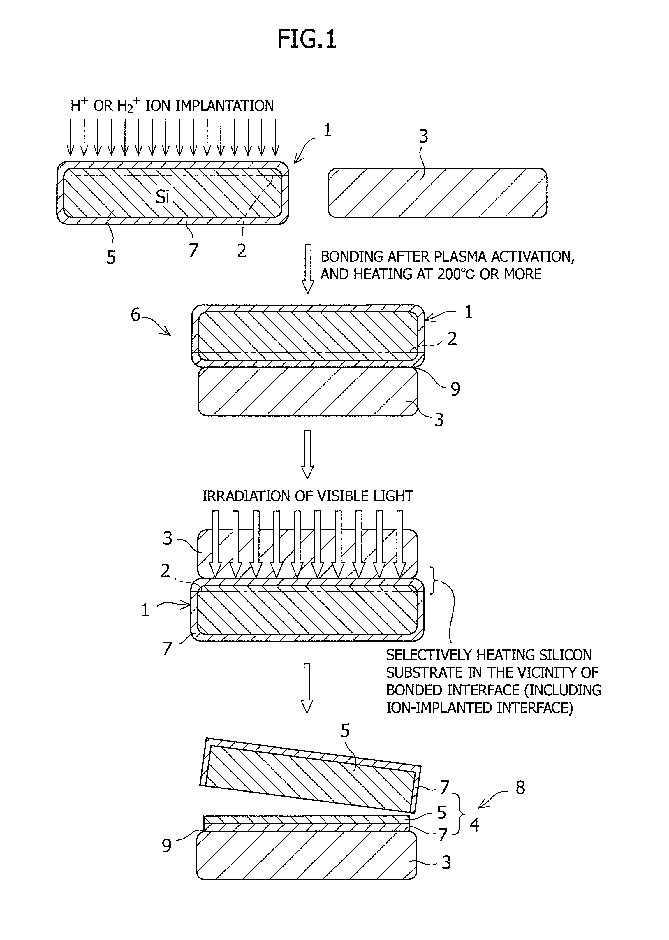
[0072]A silicon substrate (thickness 625 μm) having a diameter of 150 mm on which an oxide film had been grown to 200 nm was subjected to implantation of hydrogen ions at 37 keV and a dose amount of 6.0×10¹⁶ atoms / cm2. Both surfaces of a sapphire substrate was subjected to ion beam activation treatment. Then the silicon substrate was bonded to the sapphire substrate at 150° C. After the substrate was subjected to heat treatment at 225° C. for 24 hours for primary bonding, a bonded wafer was heated to 200° C. and irradiated with a green laser having a wavelength of 532 nm from a sapphire substrate side. A laser condition at this time was 20 J / cm2. After the overall surface of the substrate was irradiated, a silicon film was transferred onto the sapphire substrate by splitting along a bonded interface to which a mechanical impact was applied. The transfer of the silicon film onto the overall surface of the substrate could be confirmed. The silicon layer of the substrate was made to a ...

example 2

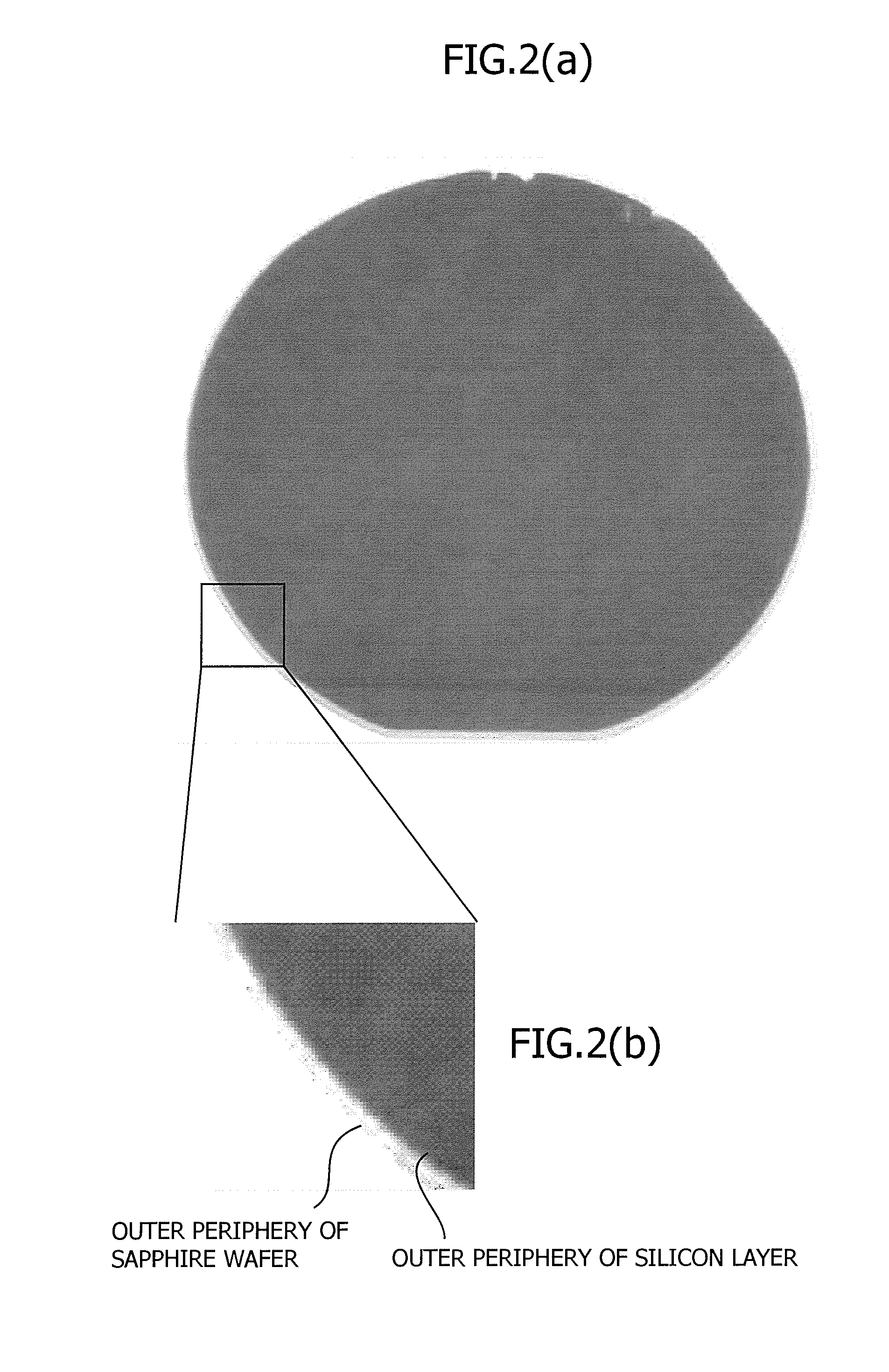
[0073]A silicon substrate (thickness 625 μm) having a diameter of 150 mm on which an oxide film had been grown to 200 nm was subjected to hydrogen ions at 37 keV and a dose amount of 6.0×10¹⁶ atoms / cm2. Both surfaces of a sapphire substrate were subjected to plasma activation treatment. Then the silicon substrate was bonded to the sapphire substrate at 200° C. After the substrate was subjected to heat treatment at 225° C. for 24 hours for primary bonding, light from a xenon flash lamp was irradiated from the sapphire substrate side at 250° C. After the overall surface of the substrate was irradiated, a silicon film was transferred to the sapphire substrate by splitting along a bonded interface to which a mechanical impact was applied. The transfer of the silicon film onto the overall surface of the substrate could be confirmed. When the silicon layer of the substrate was subjected to CPM polishing and made to a thickness of 50 nm. The number of defects of the central part and the ou...

example 3

[0075]A silicon substrate (thickness 625 μm) which having a diameter of 150 mm on which an oxide film had been grown to 200 nm was subjected to implantation of hydrogen ions at 37 keV and a dose amount of 6.0×10¹⁶ atoms / cm2. Both surfaces of a sapphire substrate was subjected to UV ozone activation treatment. Then the silicon substrate was bonded to the sapphire substrate at 100° C. After the substrate was subjected to heat treatment at 225° C. for 24 hours for primary bonding, light from a xenon flash lamp was irradiated from the sapphire substrate side at 175° C. After the overall surface of the substrate was irradiated, a silicon film was transferred to the sapphire substrate by splitting along a bonded interface to which a mechanical impact was applied. Cross-sectional TEM (transmission electron microscope) photographs of the substrate were taken at two positions, i.e., at a center and on an outer periphery. No defect was observed at all in a field of view having a narrow TEM le...


PUM


Abstract

A bonded SOS substrate having a semiconductor film on or above a surface of a sapphire substrate is obtained by a method with the steps of implanting ions from a surface of a semiconductor substrate to form an ion-implanted layer; activating at least a surface from which the ions have been implanted; bonding the surface of the semiconductor substrate and the surface of the sapphire substrate at a temperature of 50° C. to 350° C.; heating the bonded substrates at a maximum temperature from 200° C. to 350° C. to form a bonded body; and irradiating visible light from a sapphire substrate side or a semiconductor substrate side to the ion-implanted layer of the semiconductor substrate for embrittling an interface of the ion-implanted layer, while keeping the bonded body at a temperature higher than the temperature at which the surfaces of the semiconductor substrate and the sapphire substrate were bonded.

Description

BACKGROUND OF THE INVENTION[0001]1. Field of the Invention[0002]The invention relates to an SOS substrate having a low defect density in the vicinity of an interface.[0003]2. Description of Related Art[0004]Conventionally, a silicon-on-sapphire (SOS) substrate containing sapphire having a high insulation property, a low dielectric loss and a high thermal conductivity as a handle substrate has come into practical use since 1960s. The SOS substrate is an oldest silicon-on-insulator (SOI) substrate and forms an SOI structure by heteroepitaxially growing silicon on an R surface (1012) of sapphire.[0005]However, recently, an SOI using a SIMOX method, the bonding method and the like has become a main stream. Although the SOS substrate, which is an SOI substrate having silicon on a sapphire substrate, cannot cope, the SOS substrate has been used only for a device such as a high frequency device requiring a low dielectric loss. It is known that since a heteroepitaxial SOS substrate is forme...

Claims


Application Information

Patent Timeline
IPC IPC(8): H01L29/02H01L21/762
CPCH01L21/76254H01L21/268
Inventor AKIYAMA, SHOJIITO, ATSUOTOBISAKA, YUJIKAWAI, MAKOTO
Owner SHIN ETSU CHEM IND CO LTD
Why Eureka
Try Eureka