N-type organic thin film transistor, ambipolar field-effect transistor, and method of fabricating the same

a technology which is applied in the field of n-type organic thin film transistor and ambipolar field effect transistor, can solve the problems of poor reliability and unstable air of organic thin film transistor, and achieve the effect of higher electron mobility

Inactive Publication Date: 2012-07-12
NATIONAL TSING HUA UNIVERSITY
View PDF1 Cites 13 Cited by
  • Summary
  • Abstract
  • Description
  • Claims
  • Application Information

AI Technical Summary

Benefits of technology

[0044]According to the present invention, in the ambipolar field-effect transistor, the substrate can be one selected from a group consisted of: a plastic substrate (or other flexible substrate), a glass substrate, a quartz substrate, a silicon substrate, and a paper substrate, but is not limited thereto. Preferably, the substrate is a flexible substrate, i.e. a plastic substrate or a paper substrate. When the plastic substrate or paper substrate is used, the ambipolar field-effect transistor prepared in the present invention has flexibility. The material of each electrode containing the gate electrode, the source electrode, and the drain electrode may be independently selected from a group consisting of Al, Cu, Ni, Mg, Ca, Li, Cr, Ag, Pt, Au, ZnO, ITO (indium tin oxide), IZO (indium zinc oxide), AZO (aluminium zinc oxide), IGZO (indium gallium zinc oxide), etc.
[0045]According to the present invention, in the ambipolar field-effect transistor, the gate-insulating layer preferably has a single-layered structure or a multi-layered structure. The thickness of the overall gate-insulating layer can be adjusted with the number of the individual layers added, so as to obtain higher electron mobility.

Problems solved by technology

However, the fullerene thin film is not compact enough and therefore water or oxygen may be easily diffused into fullerene thin film, which means the resultant OTFT (organic thin film transistor) is unstable in the air, has poor reliability, and has low commercial value.
However, the fullerene (C60) thin film is not compact enough and is not stable in the air, and therefore the reliability of the OTFT cannot be improved and the commercial value cannot be increased.

Method used


Image

  • N-type organic thin film transistor, ambipolar field-effect transistor, and method of fabricating the same
  • N-type organic thin film transistor, ambipolar field-effect transistor, and method of fabricating the same
  • N-type organic thin film transistor, ambipolar field-effect transistor, and method of fabricating the same

Examples


example 1

Top Contact N-Type OTFT

[0085][Preparation of a Silk Solution]

[0086]First, 10 wt % of an aqueous solution of Na2CO3 was provided and heated. When the solution was boiling, natural silk was added thereto, and the solution was kept boiling to remove sericin. Then, the silk without sericin was washed by deionized water to remove the alkali salt adhered on the silk. After a drying process, refined silk, i.e. fibroin, was obtained.

[0087]Next, the refined silk was added into 85 wt % of phosphoric acid (H3PO4) solution (20 ml), and the resulted solution was stirred until the refined silk was dissolved. Then, the phosphoric acid solution containing the refined silk was put into a membrane (Spectra / Por 3 membrane, molecular weight cutoff=14000). A dialysis process was performed for 3 days to remove the phosphoric acid. Besides removing the phosphoric acid, the final pH value of the fibroin solution may also be controlled by adjusting the volume and the number of times the filtering is perform...

example 2

Bottom-Contact N-Type OTFT

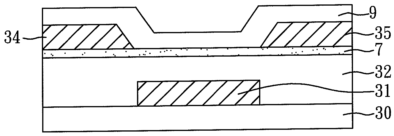
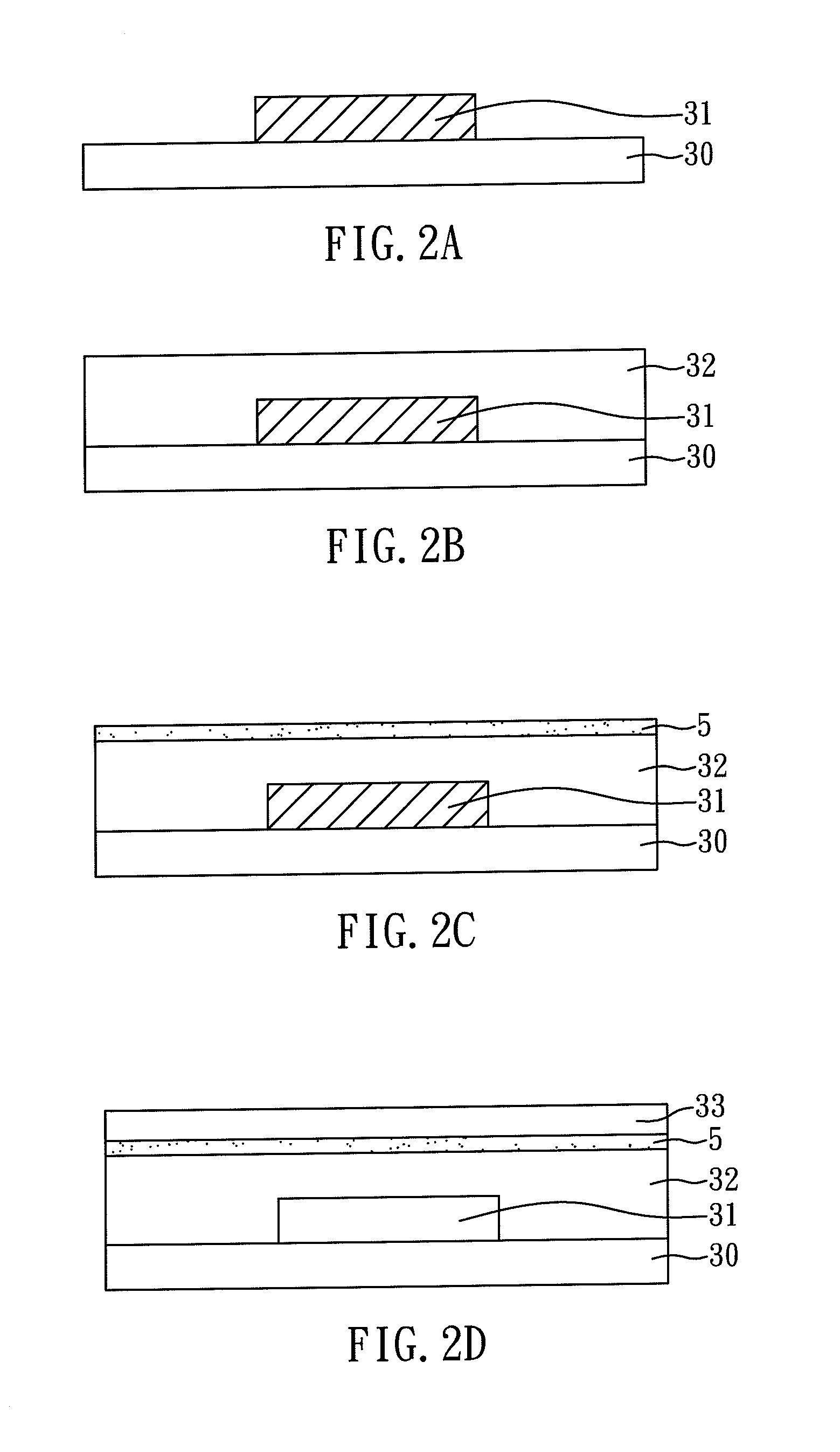
[0107]As shown in FIG. 5A, a substrate 30 was provided, and a gate electrode 31 and a gate insulating layer 32 was formed on the substrate 30 sequentially. In the present example, the preparing methods and the materials of the substrate 30, the gate electrode 31, and the gate-insulating layer 32 are the same as those illustrated in example 1. In addition, in the present example, the thickness of the gate electrode 31 was about 80 nm, and the thickness of the gate-insulating layer 32 was about 400 nm.

[0108]Next, the evaporation process was performed on the gate insulating layer 32 to form a patterned metal layer through the same evaporation process for forming the gate electrode described in Example 1, wherein the patterned metal layer was used as a source electrode 34 and a drain electrode 35, as shown in FIG. 5B. In the present example, the material of the source electrode 34 and the drain electrode 35 was Au, and the thickness of the source electrode 34 a...

example 3

Top Contact Ambipolar Field-Effect Transistor

[0112]As shown in FIG. 6A, a substrate 30 was provided, and a gate electrode 31 and a gate insulating layer 32 was formed on the substrate 30 sequentially. In the present example, the preparing methods and the materials of the substrate 30, the gate electrode 31, and the gate-insulating layer 32 are the same as those illustrated in example 1. In addition, in the present example, the thickness of the gate electrode 31 was about 80 nm, and the thickness of the gate-insulating layer 32 was about 400 nm.

[0113]Then, as shown in FIG. 6B, a P-type organic semiconductor layer 7 was formed on the gate insulating layer 32 using the same method for forming the buffering layer described in Example 1, wherein the material of the P-type organic semiconductor layer 7 was pentacene, and the thickness of the P-type organic semiconductor layer 7 was about 10 nm.

[0114]Next, as shown in FIG. 6C, an N-type organic semiconductor layer 9 was formed on the P-typ...


PUM

PropertyMeasurementUnit
thicknessaaaaaaaaaa
thicknessaaaaaaaaaa
thicknessaaaaaaaaaa

Abstract

An N-type organic thin film transistor, an ambipolar field-effect transistor, and methods of fabricating the same are disclosed. The N-type organic thin film transistor of the present invention comprises: a substrate; a gate electrode locating on the substrate; a gate-insulating layer covering the gate electrode, and the gate-insulating layer is made of silk protein; a buffering layer locating on the gate-insulating layer, and the buffering layer is made of pentacene; an N-type organic semiconductor layer locating on the buffering layer; and a source and a drain electrode, wherein the N-type organic semiconductor layer, the buffering layer, the source and the drain electrode are disposed over the gate dielectric layer.

Description

CROSS REFERENCE TO RELATED APPLICATION[0001]This application is a Continuation-in-Part of co-pending application Ser. No. 12 / 841,678, filed on Jul. 22, 2010, and for which priority is claimed under 35 U.S.C. §120; and this application claims priority of Application No. 100146057 filed in Taiwan on Dec. 13, 2011 under 35 U.S.C. §119, the entire contents of all of which are hereby incorporated by reference.BACKGROUND OF THE INVENTION[0002]1. Field of the Invention[0003]The present invention relates to an N-type organic thin film transistor, an ambipolar field-effect transistor, and methods of fabricating the same and, more particularly, to an N-type organic thin film transistor and an ambipolar field-effect transistor using silk protein as the gate-insulating layer, and methods of fabricating the same.[0004]2. Description of Related Art[0005]As well known to those skilled in the art, transistors are applied in a wide variety of electronics to serve as switches for electric current, e....

Claims


Application Information

Patent Timeline
Patent Type & Authority Applications(United States)
IPC IPC(8): H01L51/10H01L51/40
CPCB82Y10/00H01L28/40H01L51/0046H01L51/0053H01L51/0562H01L51/0093H01L51/052H01L51/0545H01L51/0055H10K85/211H10K85/621H10K85/623H10K85/761H10K10/471H10K10/486H10K10/466
Inventor HWANG, JENN-CHANGTSAI, LI-SHIUANLEE, CHUN-YITSAI, CHENG-LUN
Owner NATIONAL TSING HUA UNIVERSITY
Why Eureka
Try Eureka