Manufacturing method of magnetic recording medium
a manufacturing method and magnetic recording technology, applied in the field of magnetic recording medium manufacturing method, can solve the problems of obstructive factor, loss of recording signal, etc., and achieve the effects of reducing the magnetic spacing, excellent corrosion resistance, and mechanical durability
- Summary
- Abstract
- Description
- Claims
- Application Information
AI Technical Summary
Benefits of technology
Problems solved by technology
Method used
Image
Examples
example 1
[0088]Amorphous aluminosilicate glass was molded into a disk shape using direct press, and a glass disk was fabricated. This glass disk was sequentially subjected to grinding, polishing, and chemical strengthening, and a smooth non-magnetic glass substrate made of a chemically strengthened glass disk was obtained. The disk diameter is 65 mm. The surface roughness of the major surface of this glass substrate was measured by AFM (atomic force microscope), and the surface shape was smooth with Rmax at 2.18 nm and Ra at 0.18 nm. Rmax and Ra comply with Japanese Industrial Standards (JIS).
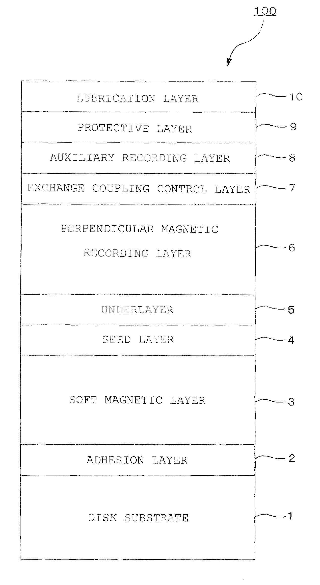
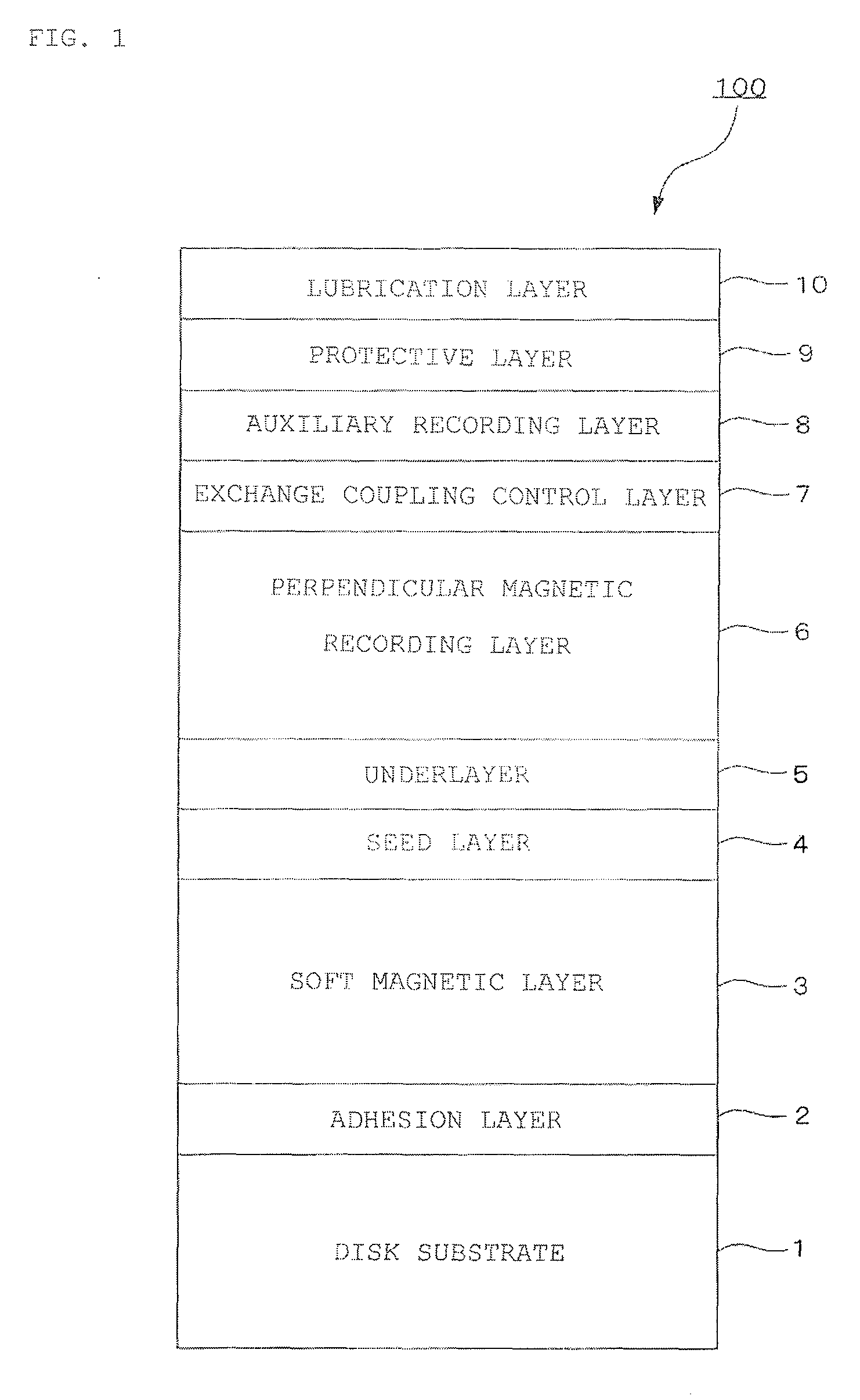
[0089]Subsequently, films of an adhesion layer, a soft magnetic layer, a seed layer, an underlay first layer, an underlay second layer, a perpendicular magnetic recording layer, an exchange coupling control layer and an auxiliary recording layer are sequentially formed on the glass substrate by using a leaf-type static opposing sputtering device with a DC magnetron sputtering method.
[0090]The following ...
example 2
[0103]In the film-forming process of the protective layer in Example 1, the protective layer was formed similarly to Example 1 except that a 0.9-nm film of the CH layer was formed at the gas pressure of 3.5 Pa and then, a 1.8-nm film of the CH layer was formed at the gas pressure of 0.9 Pa, and after that, a 0.3-nm film of the CHN layer was formed so as to have the total film thickness of the protective layer of 3 nm.
[0104]The magnetic disk was fabricated similarly to Example 1 except for that point, and the magnetic disk of Example 2 was obtained.
example 3
[0105]In the film-forming process of the protective layer in Example 1, the protective layer was formed similarly to Example 1 except that a 0.9-nm film of the CH layer was formed at the gas pressure of 3.5 Pa and then, a 1.9-nm film of the CH layer was formed at the gas pressure of 0.9 Pa, and after that, a 0.7-nm film of the CHN layer was formed so as to have the total film thickness of the protective layer of 3.5 nm.
[0106]The magnetic disk was fabricated similarly to Example 1 except for that point, and the magnetic disk of Example 3 was obtained.
PUM
| Property | Measurement | Unit |
|---|---|---|
| Thickness | aaaaa | aaaaa |
| Nanoscale particle size | aaaaa | aaaaa |
| Thickness | aaaaa | aaaaa |
Abstract
Description
Claims
Application Information


