Fabrication of lasing microcavities consisting of highly luminescent colloidal nanocrystals

a technology of colloidal nanocrystals and micro-cavities, which is applied in the direction of active medium materials, semiconductor lasers, crystal growth processes, etc., can solve the problems of difficult lasering, shortened excited state lifetime to tens of picoseconds, and difficult to achieve optical gain in colloidal semiconductor nanocrystals

Active Publication Date: 2012-08-09
FOND INST ITAL DI TECH
View PDF2 Cites 24 Cited by
  • Summary
  • Abstract
  • Description
  • Claims
  • Application Information

AI Technical Summary

Benefits of technology

[0006]The present invention provides a method for producing a lasing microdevice, wherein the colloidal nanocrystals themselves form the resonating cavity needed for the laser feedback, which removes the necessity to fabricate an external resonator. Moreover, according to the invention, the resonator is formed by a self-assembly of the light emitting nanocrystals on a micrometer scale, which opens many possibilities for large scale production of such microlasers by economic jet deposition techniques.

Problems solved by technology

So far, lasing was difficult to achieve in nanocrystals because optical gain competed with Auger recombination above threshold, which shortened excited state lifetime to tens of picoseconds,4 and laser feedback was possible only via external resonators.
The achievement of optical gain in colloidal semiconductor nanocrystals is challenging because two main obstacles have to be faced, namely trapping of excited carriers at surface / interface defect states5 and Auger recombination.
The need for an external resonator imposed several difficulties in matching the fabrication steps of wet chemical synthesis and deposition with the processes needed to fabricate the resonator.

Method used


Image

  • Fabrication of lasing microcavities consisting of highly luminescent colloidal nanocrystals
  • Fabrication of lasing microcavities consisting of highly luminescent colloidal nanocrystals
  • Fabrication of lasing microcavities consisting of highly luminescent colloidal nanocrystals

Examples


Embodiment Construction

Experimental Section

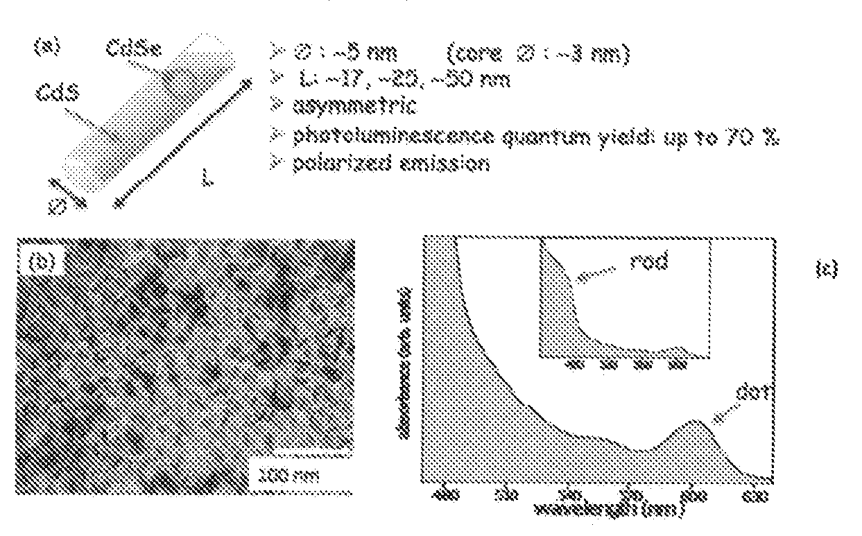
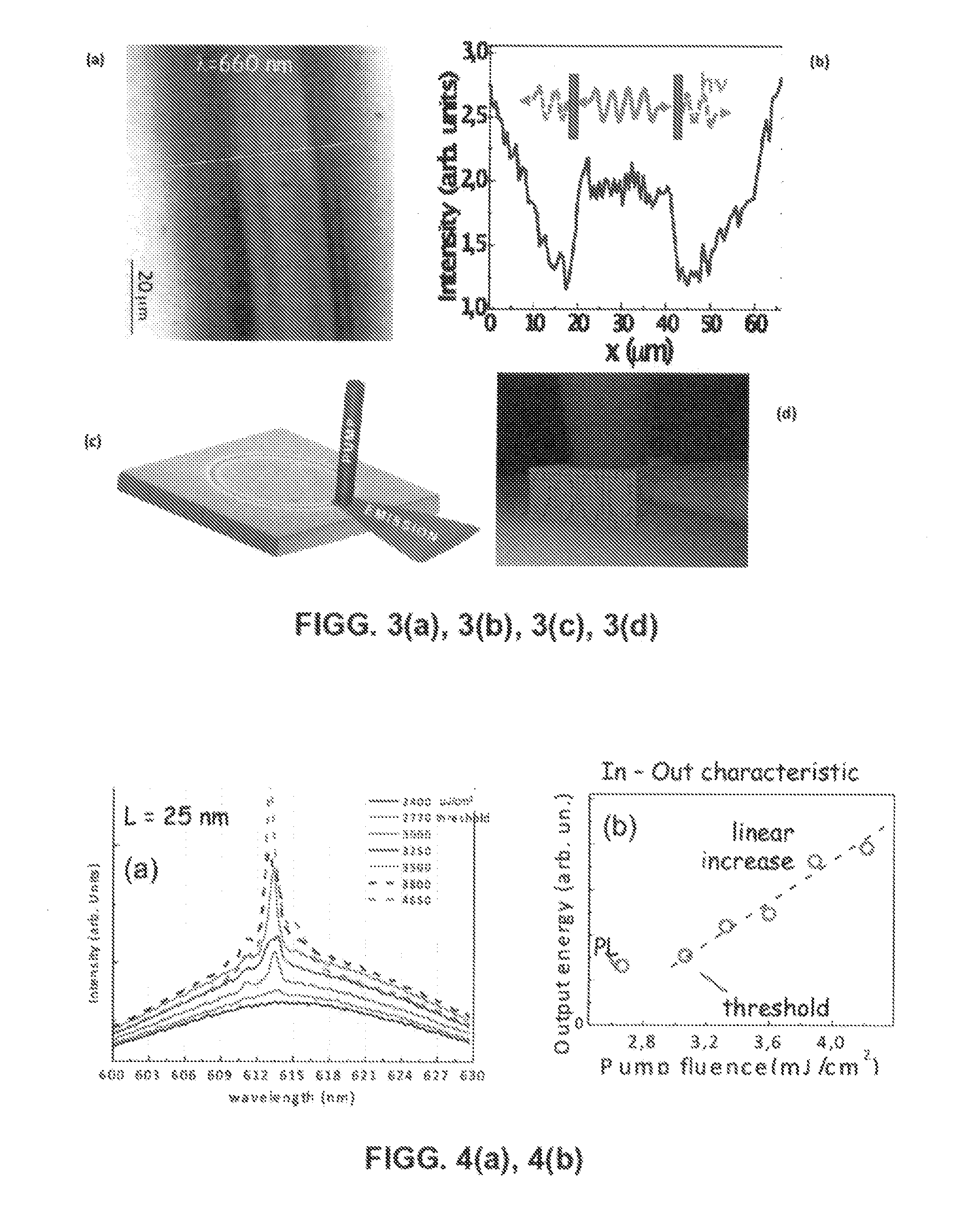
[0043]Colloidal core-shell CdSe / CdS nanorods were obtained by the seeded growth method, published by L. Carbone et al. in Nano Letters, 2007, 7, 2942-2950. The obtained nanorods, which are soluble in toluene in a concentration of 1-3 μM, exhibit both high fluorescent quantum yields (up to 70%) and linear polarized emission. The emission wavelength of the nanorods is in the range of 600-630 nm, but can in principle be controlled over a spectral window from 570 nm to 650 nm.

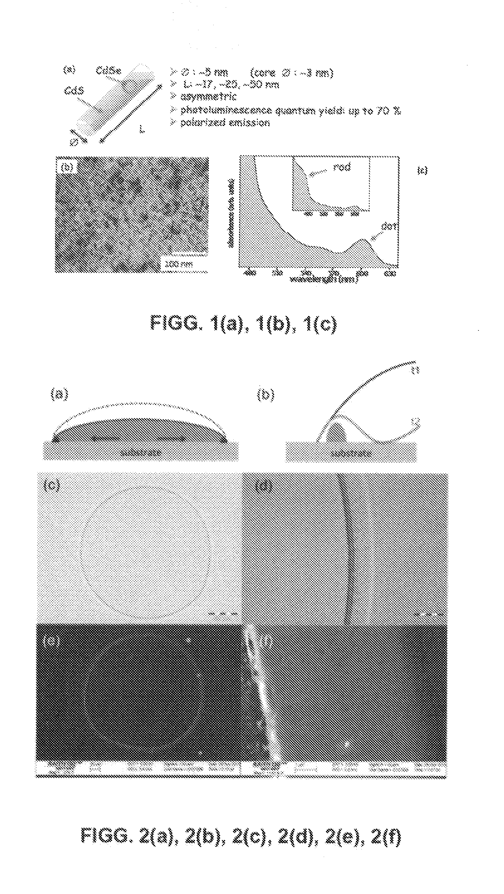
[0044]The nanorods were dissolved in toluene at a concentration of 10−6 M. The obtained solution was jet-deposited by means of a capillary with 20 μm diameter on a previously cleaned glass slide (cleaning by 20 min ultrasonic in acetone and 20 min ultrasonic in propanol, and low dry by nitrogen). The jet-deposition was performed using a Femtojet (Eppendorf) system combined with an inverted optical microscope. The capillary-glass slide distance was adjusted to some hundreds of microns, which corr...


PUM

PropertyMeasurementUnit
volumeaaaaaaaaaa
volumeaaaaaaaaaa
lengthaaaaaaaaaa

Abstract

A method of producing a lasing microsource of colloidal nanocrystals. The method includes the steps of preparing a nanocrystal solution in a solvent; depositing at least a drop of the nanocrystals solution with a drop volume below 1 nl on a flat substrate; and evaporating the solvent to dryness thereby to obtain at the edge of the evaporated drop a single annular stripe including a domain wherein the nanocrystals are arranged in an ordered array, wherein the ordered nanocrystals in the domain constitute an active region capable of lasing and the radially inner and outer edges of the stripe define a resonant cavity in which the active region is inserted.

Description

BACKGROUND OF THE INVENTION[0001]The present invention relates to the production of lasing microdevices and specifically to self-assembled lasing microcavities consisting of highly luminescent nanocrystals.[0002]Colloidal semiconductor nanocrystals have been exploited in electro-optical devices like light emitting diodes,1 lasers2, 3 and solar cells. This trend is driven by the advanced synthesis of nanocrystals of various materials, sizes and shapes and will benefit from progress in their organization into ordered architectures by self-assembly. So far, lasing was difficult to achieve in nanocrystals because optical gain competed with Auger recombination above threshold, which shortened excited state lifetime to tens of picoseconds,4 and laser feedback was possible only via external resonators.[0003]The achievement of optical gain in colloidal semiconductor nanocrystals is challenging because two main obstacles have to be faced, namely trapping of excited carriers at surface / interf...

Claims


Application Information

Patent Timeline
Patent Type & Authority Applications(United States)
IPC IPC(8): H01S3/06C30B19/00C30B7/02
CPCB82Y20/00C30B7/02H01S5/3412H01S3/169C30B29/605
Inventor KRAHNE, ROMANMANNA, LIBERATOZAVELANI-ROSSI, MARGHERITALANZANI, GUGLIELMOGIRARDO, SALVATOREPISIGNANO, DARIOLUPO, MARIA GRAZIA
Owner FOND INST ITAL DI TECH
Why Eureka
Try Eureka