Semiconductor memory device and method of manufacturing semiconductor memory device

a semiconductor memory and semiconductor technology, applied in semiconductor devices, digital storage, instruments, etc., can solve the problems of deterioration of the subthreshold characteristics of write transistors, insufficient consideration of an increase in the integration degree of gain cells, and difficult to achieve a cell area as small as 6 fsup>2 , etc., to reduce parasitic capacitance, reduce parasitic capacitance between the read bit line and such components, and reduce parasitic capacitance

Inactive Publication Date: 2012-08-23
SEMICON ENERGY LAB CO LTD
View PDF7 Cites 27 Cited by
  • Summary
  • Abstract
  • Description
  • Claims
  • Application Information

AI Technical Summary

Benefits of technology

[0039]In the above structure, the read bit line is provided below the first semiconductor film and a component which can be an obstacle is not particularly provided in that portion, so that the depth at which the read bit line is arranged can be set as appropriate. Needless to say, the read bit line can be formed apart from the transistor (that is, in a deep position) to further reduce the parasitic capacitance. Further, the depth of one read bit line is set to be different from the depth of another read bit line adjacent thereto, whereby the parasitic capacitance generated between the adjacent read bit lines can also be reduced.
[0040]Furthermore, since the read bit line is positioned apart from the capacitor, the write word line, and the like, the parasitic capacitance between the read bit line and such components can also be reduced and signal delay can be suppressed.
[0041]By providing a circuit for driving the read bit line below the read bit line, the chip area can be reduced. In general, a driver circuit occupies 20% to 50% of a surface of a DRAM chip, which also applies to the gain cell. When the driver circuit and a memory cell array overlap with each other, the chip area can be reduced, or a larger number of memory cells can be formed than in the case of a conventional DRAM having the same chip area. The driver circuit is preferably formed using a single crystal semiconductor.

Problems solved by technology

However, enough consideration of an increase in the integration degree of a gain cell has not been made.
Since the gain cell includes two transistors and thus needs a large area for one memory cell when the transistors are arranged in one plane, it is difficult to achieve a cell area as small as 6 F2 (F is a feature size) unlike a 1Tr-DRAM.
Further, when the circuit is miniaturized, the subthreshold characteristics of the write transistor deteriorate because of a short-channel effect and the off-state resistance thereof tends to decrease; no effective solutions for this problem have been proposed.

Method used


Image

  • Semiconductor memory device and method of manufacturing semiconductor memory device
  • Semiconductor memory device and method of manufacturing semiconductor memory device
  • Semiconductor memory device and method of manufacturing semiconductor memory device

Examples


embodiment 1

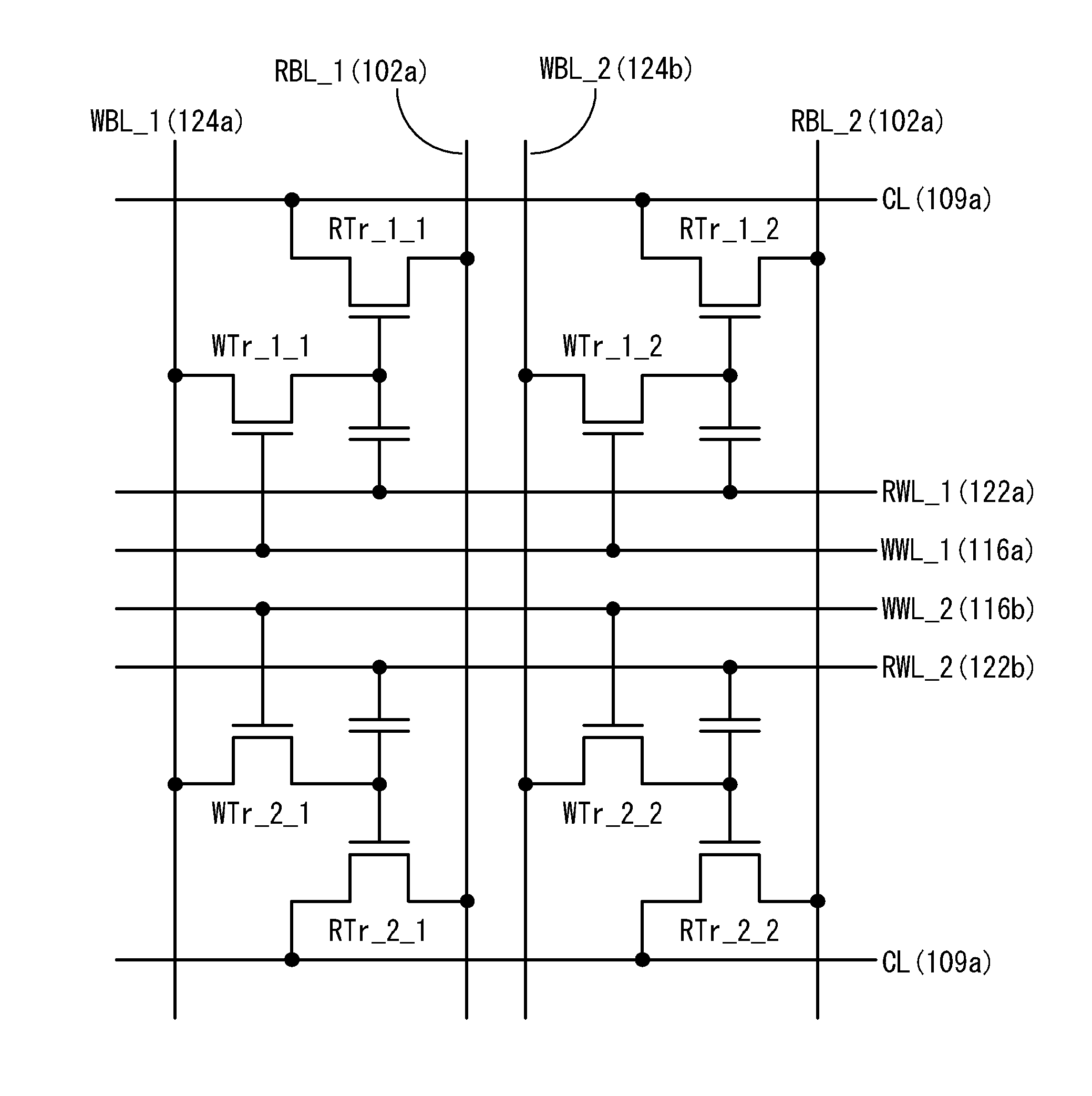
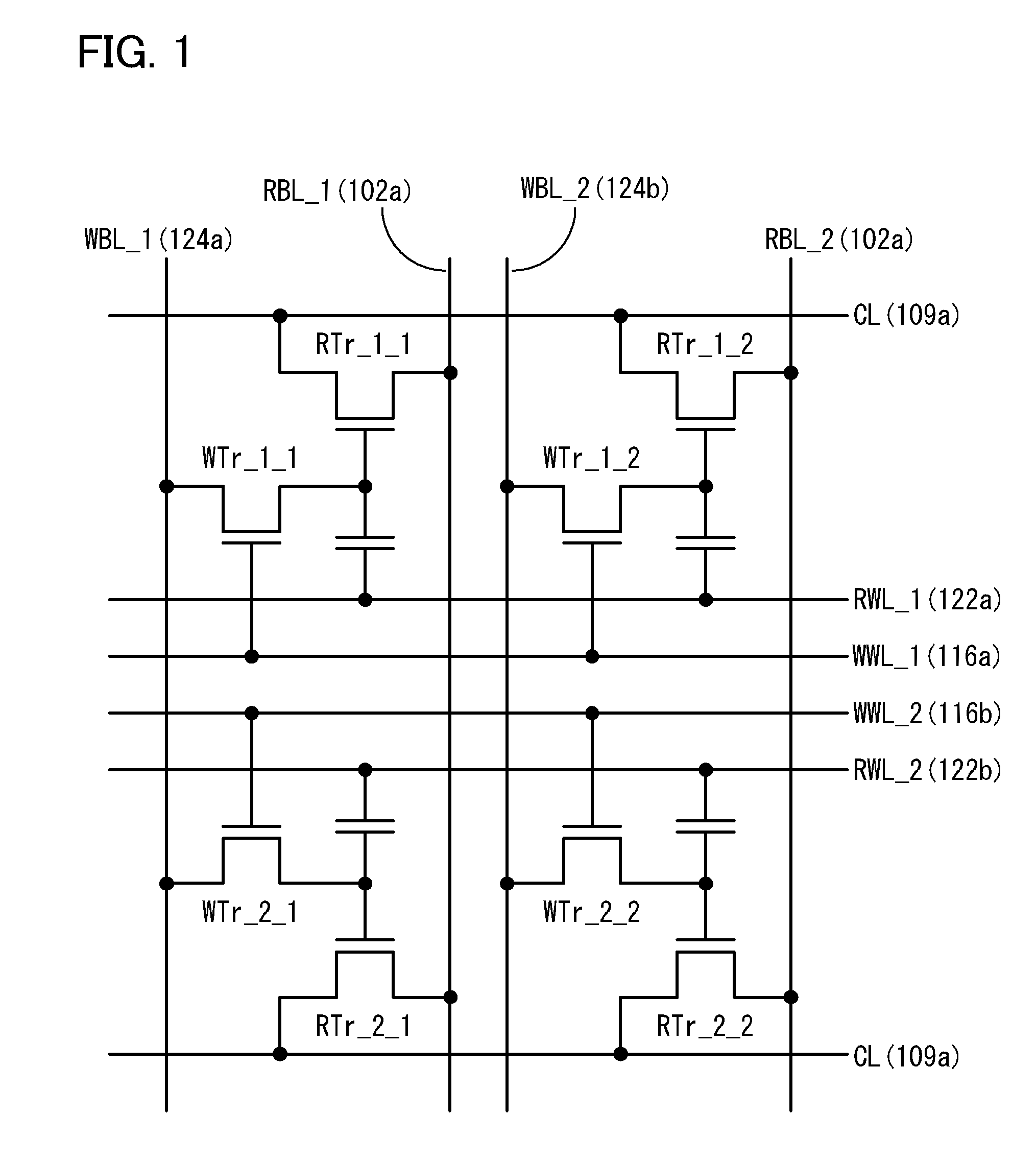
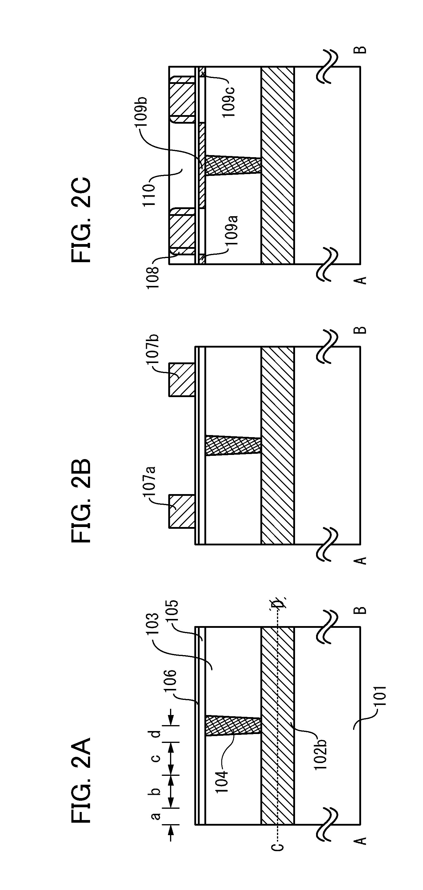
[0058]A manufacturing process of a memory cell according this embodiment will be described with reference to FIGS. 2A to 2C, FIGS. 3A to 3D, FIGS. 4A to 4C, FIGS. 5A to 5C, FIGS. 6A to 6C, and FIGS. 7A to 7C. FIGS. 2A to 2C, FIGS. 6A to 6C, and FIGS. 7A to 7C each illustrate a cross section parallel to a bit line in the memory cell according to this embodiment. FIGS. 4A to 4C and FIGS. 5A to 5C are schematic views each illustrating a manufacturing step in the case where the memory cell according to this embodiment is seen from the above. Note that an insulating film or the like is not illustrated in FIGS. 4A to 4C and FIGS. 5A to 5C. Cross sections along dotted line A-B in FIGS. 4A to 4C and FIGS. 5A to 5C correspond to FIGS. 2A to 2C, FIGS. 6A to 6C, and FIGS. 7A to 7C.

[0059]In this embodiment, with a few exceptions, just the outline is described. Known techniques for forming a semiconductor integrated circuit or the like may be referred to for the details. FIGS. 2A to 2C, FIGS. 6A...

embodiment 2

[0117]This embodiment will be described with reference to FIG. 8. In this embodiment, a circuit (a driver circuit 202) for driving a memory cell, such as a sense amplifier or a decoder, is formed on a surface of a substrate 201 of a single crystal semiconductor by known techniques for forming a semiconductor integrated circuit. A read bit line 203 is formed over the driver circuit 202, and a memory cell layer 204 including a write word line and a read word line is provided over the read bit line 203. Further, a write bit line 205 is formed over the memory cell layer 204.

embodiment 3

[0118]A manufacturing process of a memory cell according this embodiment will be described with reference to FIGS. 9A to 9C and FIGS. 10A to 10C. FIGS. 9A to 9C and FIGS. 10A to 10C are cross-sectional views illustrating the manufacturing process of the memory cell according to this embodiment. In this embodiment, with a few exceptions, just the outline is described. Embodiment 1, known techniques for forming a semiconductor integrated circuit, or the like may be referred to for the details. FIGS. 9A to 9C and FIGS. 10A to 10C will be described below in this order.

9A>

[0119]A read bit line 302 is formed over a first insulator 301. Further, a second insulator 303 is formed over the read bit line 302 to have an appropriate thickness. The thickness of each of the first insulator 301 and the second insulator 303 is preferably 100 nm to 1 μm. In addition, the first insulator 301 and the second insulator 303 may each be formed using a material having a relatively low permittivity such as s...


PUM


Abstract

A highly integrated gain cell-type semiconductor memory is provided. A first insulator, a read bit line, a second insulator, a third insulator, a first semiconductor film, first conductive layers, and the like are formed. A projecting insulator is formed thereover. Then, second semiconductor films and a second gate insulating film are formed to cover the projecting insulator. After that, a conductive film is formed and subjected to anisotropic etching, so that write word lines are formed on side surfaces of the projecting insulator. A third contact plug for connection to a write bit line is formed over a top of the projecting insulator. With such a structure, the area of the memory cell can be 4 F2 at a minimum.

Description

BACKGROUND OF THE INVENTION[0001]1. Field of the Invention[0002]The present invention relates to a semiconductor memory device.[0003]2. Description of the Related Art[0004]A dynamic random access memory (1Tr-DRAM) including one capacitor and one transistor (referred to as a cell transistor) has been widely used as a typical semiconductor memory device. However, there is a requirement that the capacitance of the capacitor is not changed even when a circuit is miniaturized, and thus formation of the capacitor is becoming a major hurdle.[0005]Under such a circumstance, a gain cell including two transistors and one capacitor (e.g., see Patent Document 1) has attracted attention as a potential solution for the problem of the conventional 1Tr-DRAM for the following reason. The capacitance of the capacitor in the 1Tr-DRAM is determined by the ratio of the capacitance of the capacitor to the parasitic capacitance of a bit line. In contrast, the capacitance of the capacitor in the gain cell ...

Claims


Application Information

Patent Timeline
Patent Type & Authority Applications(United States)
IPC IPC(8): G11C11/34H01L21/8239
CPCH01L27/108H01L27/1156H01L27/10844H10B12/01H10B12/00H10B41/70
Inventor TAKEMURA, YASUHIKO
Owner SEMICON ENERGY LAB CO LTD
Why Eureka
Try Eureka