Calibration for mixed-signal integrator architecture
a mixed-signal integrator and architecture technology, applied in the field of analog front end circuits, can solve the problems of false triggers, different applications are subjected to different noise spectrums, and the threshold voltage increases the sensitivity of the system, so as to reduce the charge, increase the charge, and reduce the charge
- Summary
- Abstract
- Description
- Claims
- Application Information
AI Technical Summary
Benefits of technology
Problems solved by technology
Method used
Image
Examples
first embodiment
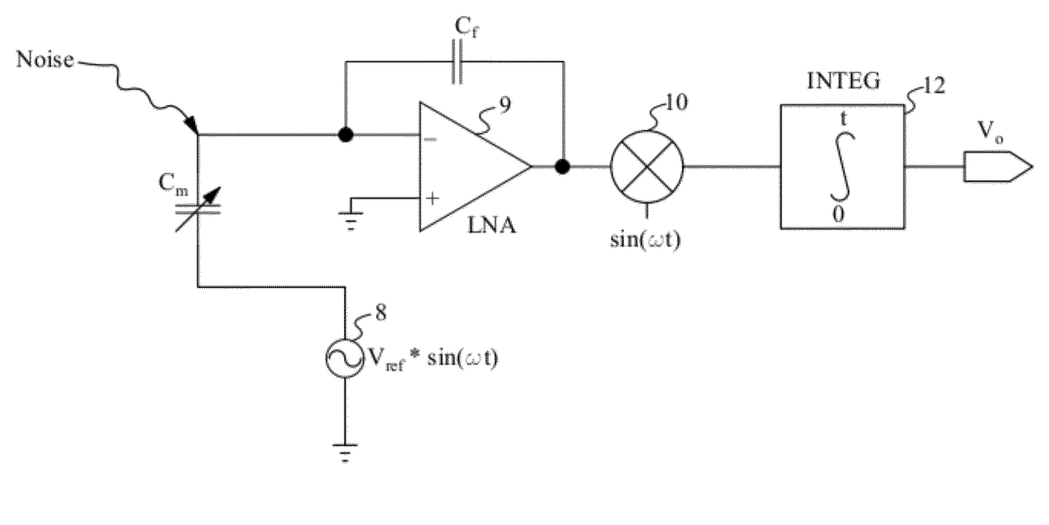
[0044]In some embodiments, a capacitance measurement is performed by an analog front end circuit that uses coherent detection, also referred to as synchronous demodulation or correlation, to reject noise and / or other interferers. FIG. 6 illustrates a simplified schematic block diagram of an analog front end circuit using coherent detection according to a Coherent detection generally refers to transmitting a signal at a certain frequency f, and detecting the signal at that same frequency f. Signals at other frequencies are considered noise. A mixer 10 and an integrator 12 are together referred to as a correlator, which performs synchronous demodulation, or correlation, to reject noise and / or interferers. In some embodiments, a mixer includes an operational amplifier and a resistor pair including a variable resistor, where an output voltage of the mixer is a function of the input voltage multiplied by the ratio of the two resistors. In some embodiments, an integrator includes an oper...
second embodiment
[0052]FIG. 9 illustrates a simplified schematic block diagram of an analog front end circuit using coherent detection according to a A programmable resistive element Rin, an amplifier 14, and an integrating feedback capacitor Ci form an integrated circuit having the combined functionality of a mixer and an integrator. The programmable resistive element is represented in FIG. 9 as Rin with an arrow. In some embodiments, the programmable resistive element Rin is implemented as a digital array of resistors, shown in the expanded area in FIG. 9 as an array of resistors R1-Rx. Each resistor R1-Rx in the array is coupled to a corresponding on-off switch S1-Sx. One or more of the resistors R1-Rx in the array can be turned on such that the overall conductance of the programmable resistive element Rin imitates a desired waveform, such as a sine wave. In this manner, an appropriate combination of resistors in the array of resistors R1-Rx can be turned on to represent the multiplication of th...
PUM
 Abstract
Description
Claims
Application Information


