Amorphous multicomponent dielectric based on the mixture of high band gap and high k materials, respective devices and manufacture

Inactive Publication Date: 2012-10-04
FACULDADE DE CIENCIAS E TECHA DA UNIV NOVA DE LISBOA +2
View PDF2 Cites 9 Cited by
  • Summary
  • Abstract
  • Description
  • Claims
  • Application Information

AI Technical Summary

Benefits of technology

[0032]Given that substrate/film bombardment can indeed be a problem in sputtering, materials with a high-κ are desirable, since their added capacitance can compensate the higher density of interface traps and thus improve transistor performance, namely decrease the subthreshold slope (S) and the operating voltage27. However, some of these dielectrics, specially the higher-κ ones, present a polycrystalline structure even if deposited at room temperature, whereas an amorphous structure is generally preferred since grain boundaries act as preferential paths for impurities diffusion and leakage current, resulting in inferior dielectric's reliability28. Besides that, amorphous materials present smoother surfaces, which can bring improved interface properties27, 28. High-κ materials have another drawback: as a general rule, higher-κ corresponds to lower bandgap (EG), hence to less favorable band offsets between the dielectric and the semiconductor, resulting in structures with low breakdown voltage and high leakage current27, 29. This is even more severe when we consider their integration with oxide semiconductors, which have a considerably higher than Si or organic semiconductors.
[0033]As a possible solution for these high-κ related issues, multicomponent dielectrics based on a mixture of Ta2O5 (high-κ, low EG) and SiO2 or Al2O3 (low-to-moderate κ, high EG) produced by sputtering at room temperature are proposed. Sputte

Problems solved by technology

The lower performance is usually consequence of less compact films and higher density of defects on the dielectric's bulk and on its interface with the oxide semiconductor.
This technique is theoretically not seen as a potential candidate for the production of reliable insulators, since dielectrics are generally very hard to sputter, leading to the usage of high power densities that might damage the growing films and interfaces.
However, some of these dielectrics, specially the higher-κ ones, present a polycrystalline structure even if deposited at room temperature, whereas an amorphous str

Method used


Image

  • Amorphous multicomponent dielectric based on the mixture of high band gap and high k materials, respective devices and manufacture
  • Amorphous multicomponent dielectric based on the mixture of high band gap and high k materials, respective devices and manufacture
  • Amorphous multicomponent dielectric based on the mixture of high band gap and high k materials, respective devices and manufacture

Examples


Embodiment Construction

Dielectric's Characterization

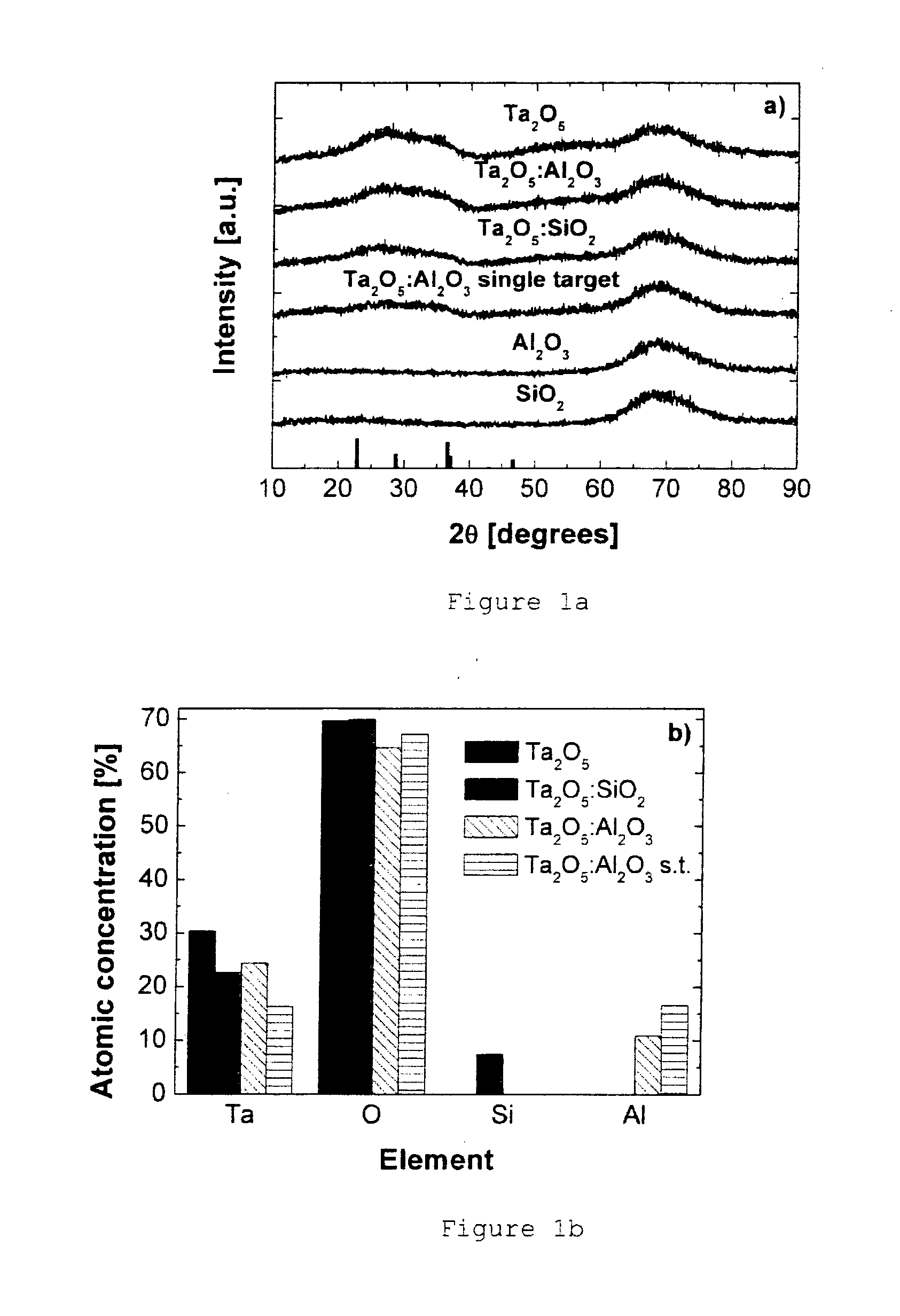
[0046]FIGS. 1a and 1b show the structural and compositional data obtained for the produced dielectrics. Note that the presented data refers to films intentionally annealed at a higher temperature (300° C.) than the one used on the TFTs (150° C.), in order to investigate the stability of their properties, namely of their structure, when subjected to higher temperatures. Concerning structural properties (FIG. 1a), the SiO2 and Al2O3 films present an amorphous structure, as expected for these large bandgap materials29. For the Ta2O5 based compositions a broad diffraction peak appears close to 2θ=30°, suggesting that some short-range order exists in the thin-films, but crystallization (i.e., long-range ordering) is not achieved.

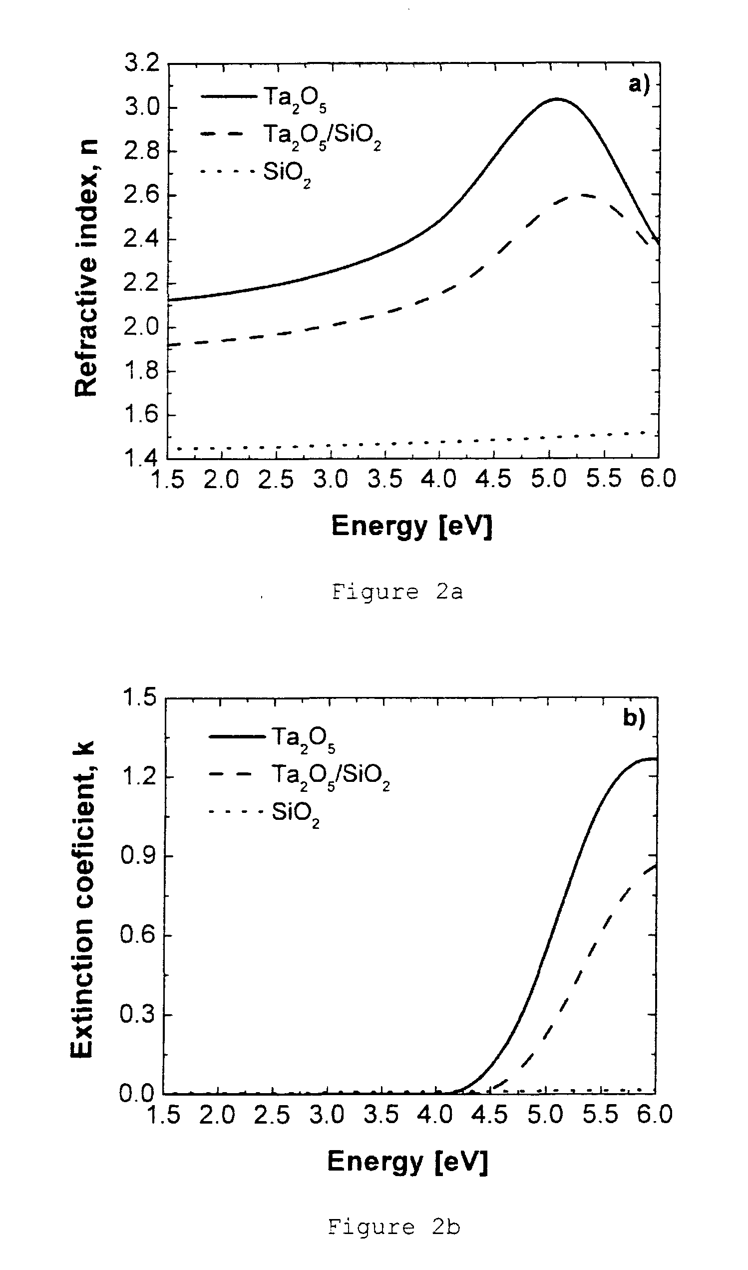
[0047]XPS and spectroscopic ellipsometry analysis suggest that this short-range order can be affected by composition, namely by the amount of Ta present in the films. According to the XPS data (FIG. 1b), Ta content is decreased from 3...


PUM


Abstract

High performance thin-film, transistors are entirely processed at temperatures not exceeding 150° C., using amorphous multi component dielectrics based on the mixture of high band gap and high dielectric constant (K) materials. The sputtered or ink jet printed mixed dielectric materials such as Ta2O5 with SiO2 or Al2O3 or HfO2 with SiO2 or Al2O3 are used. These multicomponent dielectrics allow producing amorphous dielectrics to be introduced in high stable electronic devices with low leakage currents, while preserving a high dielectric constant. This results in producing thin film transistors with remarkable electrical properties, such as the ones produced based on Ga—In—Zn oxide as channel layers and where the dielectric was the combination of the mixture Ta2O5:SiO2, exhibiting field-effect mobility exceeding 35 cm2 V−1 s−1, close to 0 V turn-on voltage, on/off ratio higher than 106 and subthreshold slope below 0.24 V dec−1.

Description

TECHNICAL FIELD[0001]Transparent electronics is one of the most fascinating and fast-growing research areas since the first fully transparent thin-film transistors (TFTs) based on ZnO were presented in 2003.1 A significant effort has been put on enhancing device's performance and lowering their maximum processing temperature2 down to at least 150° C., since this is normally seen as the upper limit for the so-called low temperature electronics, where low cost and flexible substrates are used. Besides that, we must include all silicon based CMOS technology demanding for use of high k dielectrics exhibiting very low leakage current highly relevant of all set of devices in micron, submicron and nanoscale ranging sizes.SUMMARY OF THE INVENTION[0002]In summary, the properties of sputtered or ink jet multicomponent thin-film dielectrics based on mixtures of high band gap and high κ such as Ta2O5 with SiO2 or Al2O3 or HfO2 with SiO2 or Al2O3 are the core of the present invention. These mate...

Claims


Application Information

Patent Timeline
IPC IPC(8): H01L21/31H01L29/786H01L33/08H01L29/02
CPCH01L21/0215H01L21/02178H01L21/02183H01L21/02194H01L29/7869H01L21/28194H01L21/31604H01L29/517H01L21/02266
Inventor DE PAIVA MARTINS, RODRIGO FERRAOCORREIA FORTUNATO, ELVIRA MARIACANDIDO BARQUINHA, PEDRO MIGUELNUNES PEREIRA, LUIS MIGUELGONCALVES, GONCALO PEDROKUSCER HROVATIN, DANJELAKOSEC, MARIJA
Owner FACULDADE DE CIENCIAS E TECHA DA UNIV NOVA DE LISBOA
Why Eureka
Try Eureka