Transparent conductive film, process for producing same, and electronic device employing transparent conductive film

Inactive Publication Date: 2012-11-22
LINTEC CORP
View PDF11 Cites 25 Cited by
  • Summary
  • Abstract
  • Description
  • Claims
  • Application Information

AI Technical Summary

Benefits of technology

[0032]The present invention enables provision of a transparent conductive film which has excellent transparency and conductivity and which exhibits excellent gas barrier performance and low sheet resistivity, even after having been placed in moist and high-temperature conditions.
[0033]According to the production method of the present invention, a transparent conductive film which exhibits excellent gas barrier performance can be produc

Problems solved by technology

However, since plastic film is more permeable by water vapor, oxygen, or the like than glass plate, elements in a display device tend to be damaged, which is problematic.
Therefore, when the substrate is wound or bent, cracking occurs in the gas barrier layer, and gas barrier performance is problematically degraded.
However, in the above method, satisfactory gas barrier performance can be ensured only when the thickness of the gas barrier layer is adjusted to some microns, which is problematic.
Since ITO contains indium, which is a rare metal, in recent years, a zinc oxide-based conductive material has been proposed as an ITO conductive material substitute.. However, the sheet resistivity of a zinc oxide-based conductive material under moist and high-temperature conditions dete

Method used


Image

  • Transparent conductive film, process for producing same, and electronic device employing transparent conductive film
  • Transparent conductive film, process for producing same, and electronic device employing transparent conductive film
  • Transparent conductive film, process for producing same, and electronic device employing transparent conductive film

Examples


example 1

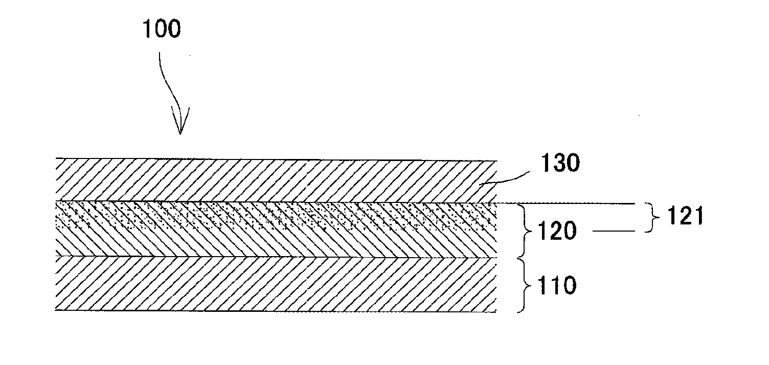
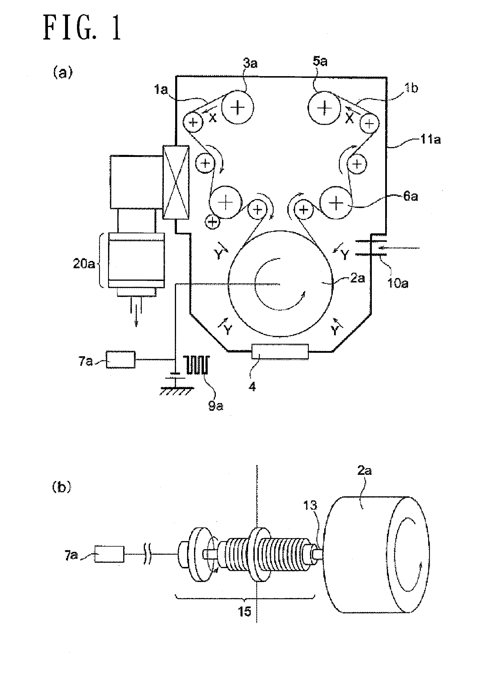
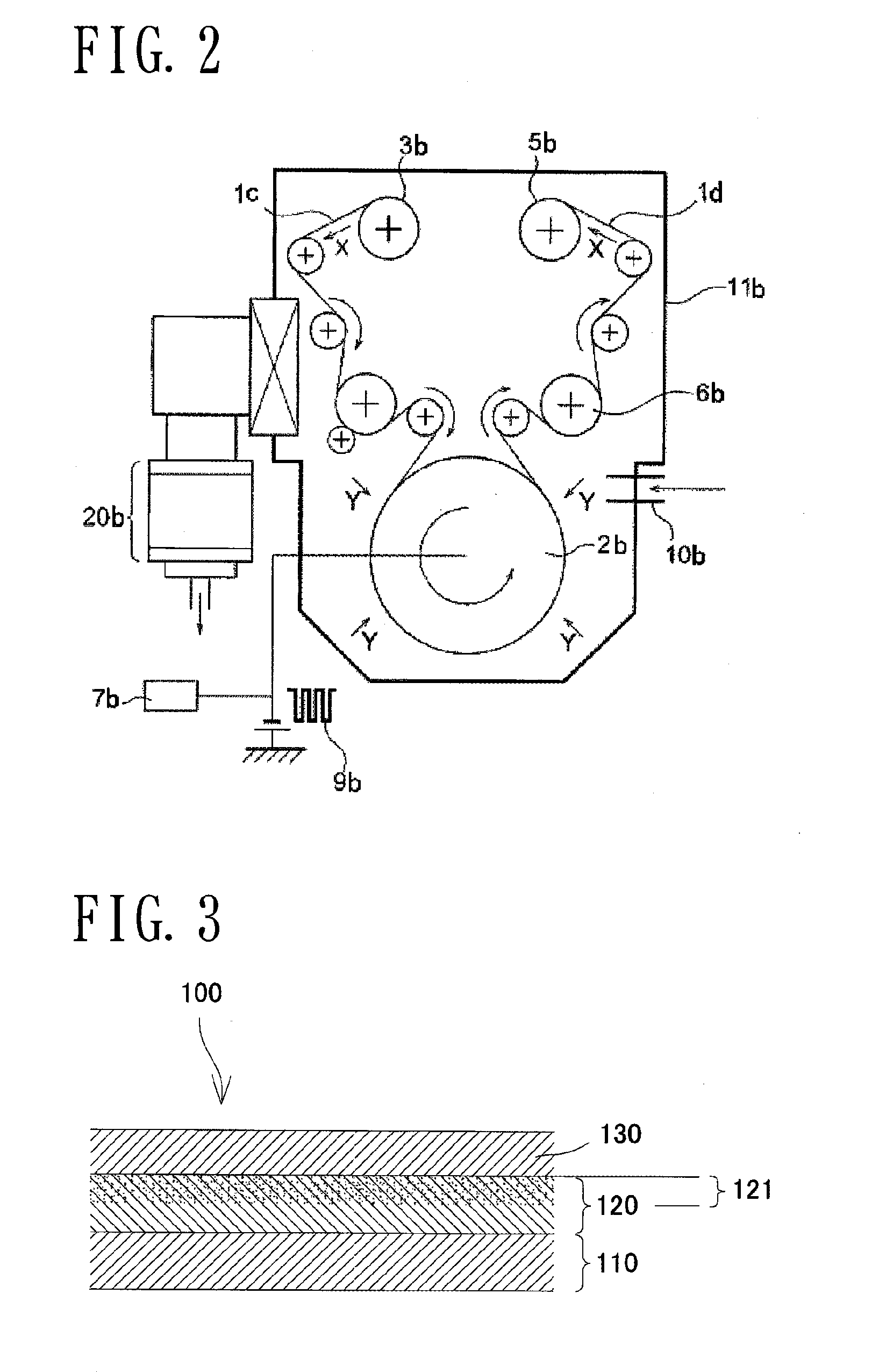
[0190]Polyethylene terephthalate film (PET188 A-4300, product of Toyobo, thickness: 188 μm) (hereinafter referred to as PET film) was employed as a substrate. A polysilazane compound (A) was applied onto the substrate and heated at 120° C. for one minute, to thereby form a layer containing perhydropolysilazane and having a thickness of 60 nm (film thickness) on the PET film. Subsequently, argon (Ar) ions were implanted through plasma ion implantation into the surface of the layer containing perhydropolysilazane by means of the plasma ion implantation apparatus shown in FIG. 1, to thereby form a gas barrier layer.

[0191]Plasma ion implantation was performed under the following conditions.[0192]Plasma-generating gas: Ar[0193]Gas flow rate: 100 sccm[0194]Duty ratio: 0.5%[0195]Repetition frequency: 1,000 Hz[0196]Applied voltage: −10 kV[0197]RF power source: frequency 13.56 MHz, applied power 1,000 W[0198]Chamber pressure: 0.2 Pa[0199]Pulse width: 5 μsec[0200]Process time (ion implantatio...

example 2

[0208]The procedure of Example 1 was repeated, except that the heating time was change from 1 minute to 5 minutes, to thereby form a transparent conductive film of Example 2.

example 3

[0209]The procedure of Example 2 was repeated, except that the thickness of the layer containing perhydropolysilazane formed on the PET film was change from 60 nm to 100 nm, to thereby form a transparent conductive film of Example 3.


PUM

PropertyMeasurementUnit
Fractionaaaaaaaaaa
Fractionaaaaaaaaaa
Fractionaaaaaaaaaa

Abstract

Disclosed is a transparent conductive film, including a substrate and, formed on at least one surface of the substrate, a gas barrier layer and a transparent conductive layer, wherein the gas barrier layer is formed of a material containing at least oxygen atoms, nitrogen atoms, and silicon atoms, and includes a surface layer part which has an oxygen atom fraction of 60 to 75%, a nitrogen atom fraction of 0 to 10%, and a silicon atom fraction of 25 to 35%, each atom fraction being calculated with respect to the total number of the oxygen atoms, nitrogen atoms, and silicon atoms contained in the surface layer part and which has a film density of 2.4 to 4.0 g/cm3.

Description

TECHNICAL FIELD[0001]The present invention relates to a transparent conductive film which exhibits excellent gas barrier performance and transparency, to a production method therefor, and to an electronic device employing the transparent conductive film.BACKGROUND ART[0002]Polymer formed products of such as plastic film are inexpensive materials with high workability which have generally been used in a variety of fields. Before use, a function of interest is added to such a product depending on the purpose of use.[0003]For example, film for wrapping foods or drugs is made of a gas barrier plastic film which prevents permeation of water vapor and oxygen, in order to prevent oxidation or denaturation of ingredients such as protein and oil and fat for maintaining the taste or freshness thereof.[0004]In recent years, for the purpose of realizing reduction in thickness and weight, flexibility, etc., attempts have been made to replace a glass plate with a transparent plastic film serving ...

Claims


Application Information

Patent Timeline
IPC IPC(8): B32B9/04C23C14/08H01B5/14C08J7/043C08J7/044C08J7/048
CPCC23C14/48C23C14/562C08J2483/14C08J2369/00C08J7/123C08J2367/02C08J7/047Y10T428/31663C08J7/0427C08J7/048C08J7/043C08J7/044B32B9/00H01B5/14C23C14/58
Inventor NAGAMOTO, KOICHIKONDO, TAKESHISUZUKI, YUTAIWAYA, WATARUNAGANAWA, SATOSHI
Owner LINTEC CORP
Why Eureka
Try Eureka