Compositions and Methods for Texturing of Silicon Wafers

a technology of silicon wafers and compositions, applied in the direction of liquid displacement, sustainable manufacturing/processing, other chemical processes, etc., can solve the problems of increasing the throughput of the wafer processing, reducing the processing time of some embodiments, etc., to improve the uniformity of texturing, reduce reflectivity, and high density

Inactive Publication Date: 2012-11-22
VERSUM MATERIALS US LLC
View PDF38 Cites 39 Cited by
  • Summary
  • Abstract
  • Description
  • Claims
  • Application Information

AI Technical Summary

Benefits of technology

[0006]Compositions of this invention can be used to treat silicon wafers or substrates or silicon films deposited on a different type of substrates (the terms substrate or wafer will be used interchangeably herein and in the claims to refer to all of these) in the texturing processes of this invention. The silicon wafers treated in accordance with these inventions may be used to make photovoltaic cells. Wafers subjected to compositions and/or methods of this invention may show improvement in the texturing uniformity and reduced reflectivity compared to the wafers not subjected to this treatment. Additional benefits that may be achieved with the method and/or composition of this invention may include one or more of the following: (1) the creation of pyramid structures on the surface of the wafer having high density and having an average height less than 10 μm, or less than 8 μm or less than 5 μm or less than 4 μm; (Often in the absence of the treatment in accordance with this invention, the average pyramid heights can be in excess of 10 μm.) (2) decreased reflectance of the textured surface; (3) decreased time needed to form pyramids and/or form the textured surface with low reflectance; (4) lower sensitivity of texturing quality to isopropyl alcohol concentration in the texturing process and in some embodiments texturing may be performed without any isopropyl alcohol or any other additive needed to promote texturing in the one or more texturing compositions; (5) when the pre-texturing composition and step is used in the texturing process, the need for additives in the texturing (etching) composition or etching solution to improve quality

Problems solved by technology

This results in decreased processing time for some embodiment

Method used


Image

  • Compositions and Methods for Texturing of Silicon Wafers
  • Compositions and Methods for Texturing of Silicon Wafers
  • Compositions and Methods for Texturing of Silicon Wafers

Examples


example 1

[0079]As-cut monocrystalline solar grade wafers were obtained from two different sources. These wafers were treated in various process sequences to achieve texturing on the surface.

[0080]In some of the processes of the examples, wafers were treated with a solution, herein referred to as Formulation 1 consisting of 4 wt % oxalic acid and 1.5 wt % Hostapur® SAS (purified by ion exchange) and the balance DI water.

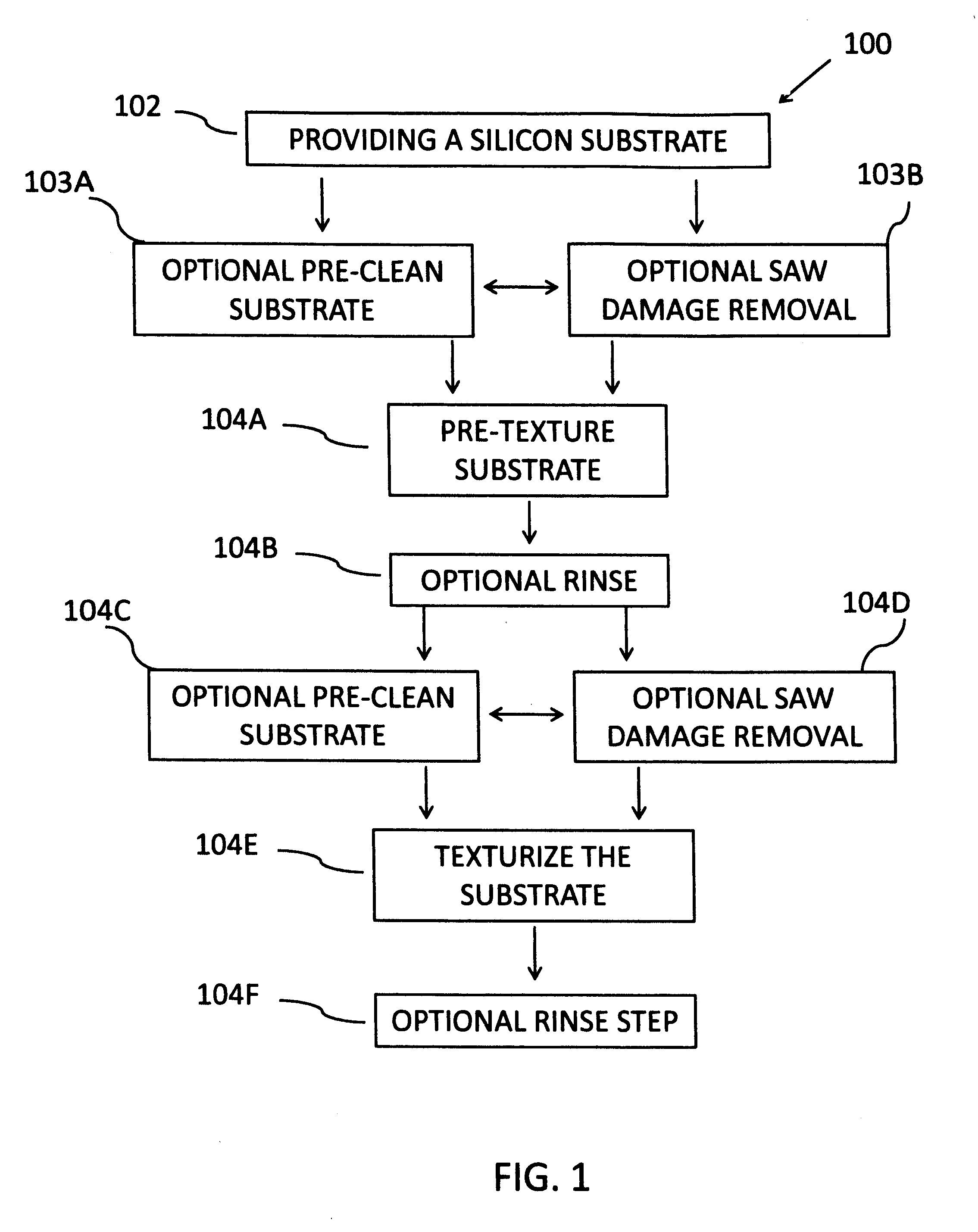
[0081]Three different texturing processes were used to process the wafer pieces. The three different processes (A, B and C) were as follows with the process steps labeled (i, ii and iii, etc) in the order in which they occurred:

[0082]Process A: (i) Saw damage removal in 20 wt % KOH solution (balance DI water) for 10 min at 80° C.; (ii) 3 min DI water rinse; (iii) texturing in a solution containing 4 wt % KOH and 2 wt % Isopropanol (IPA) (balance DI water) for 20 minutes at 80° C.; and (iv) 3 minute DI water rinse.

[0083]Process B: (i) Immersion in Formulation 1 for 5 minutes at...

example 2

[0088]As-cut monocrystalline wafers obtained from the third source were processed using Process C described for Example 1 except that the various pre-texturing formulations in Table 2 were substituted for Formulation 1 in Example 1. (Formulation 1 from Example 1 has been included in Table 2 also.)

TABLE 2Hostapur SASOxalic Acid(Purified acid form)WaterFormulation #Concentration (wt %)(wt %)(wt %)141.595.524096301.598.540.80.398.950.40.1599.45

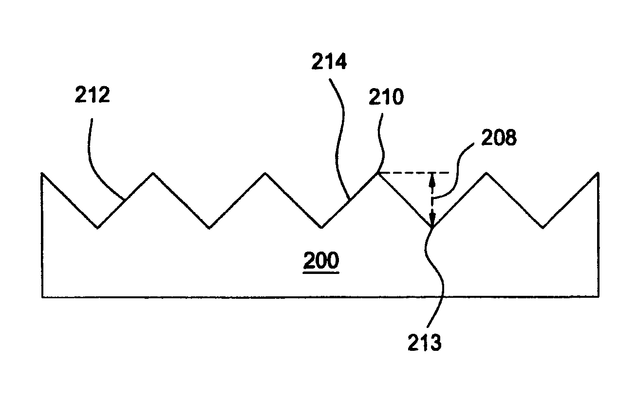
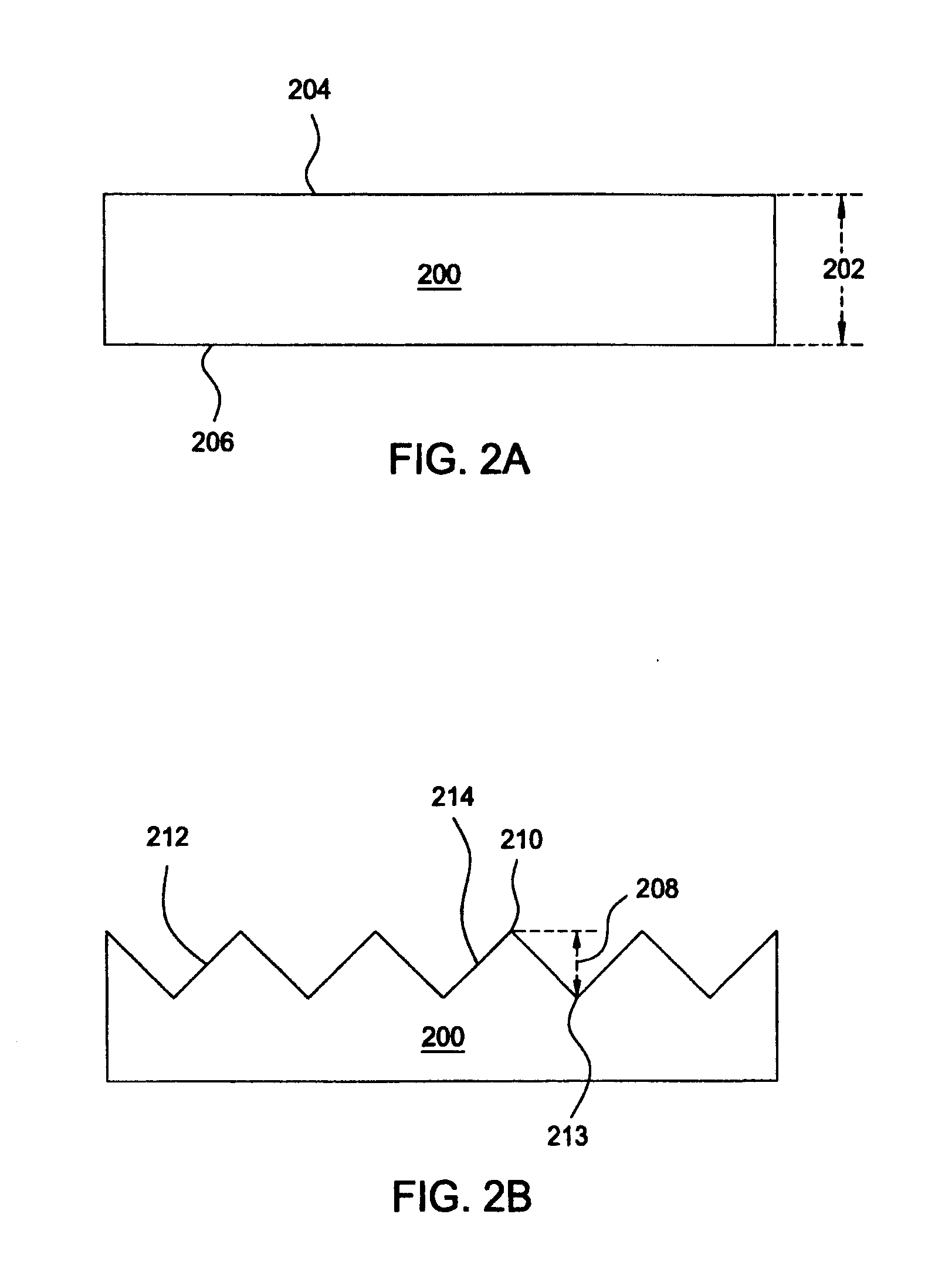
[0089]Table 3 summarizes the average reflectance percentages and the nominal pyramid heights of the wafers from Example 2 and includes the data for Formulation 1 from Example 1 also.

TABLE 3Nominal Pyramid heightFormulation #Average Reflectance (%)(μm)112.991.9215.6713.45312.114412.635.75513.1311.77

[0090]This example shows that the presence of the surfactant in the pre-texturing composition reduces reflectance and pyramid height and that more than 0.15 wt % surfactant in the pre-texturing composition may be more preferred for some embodiments.

example 3

[0091]In order to study the effect of texturing time on pyramid structures the wafers from the second source were treated using Processes A, B and C; however, the texturing times for the wafers were varied. The texturing times used were 5 minutes, 10 minutes, 15 minutes and 20 minutes for each. SEMs were taken of representative of the wafers at a 65° tilt angle treated using each of the texturing times in each Process. The SEM for the wafer treated using Process A with a 5 minute texturing step is shown in FIG. 5A. The SEM for the wafer treated using Process A with a 10 minute texturing step is shown in FIG. 5B. The SEM for the wafer treated using Process A with a 15 minute texturing step is shown in FIG. 5C. The SEM for the wafer treated using Process A with a 20 minute texturing step is shown in FIG. 5D. The SEM for the wafer treated using Process B with a 5 minute texturing step is shown in FIG. 6A. The SEM for the wafer treated using Process B with a 10 minute texturing step is ...


PUM

PropertyMeasurementUnit
Fractionaaaaaaaaaa
Fractionaaaaaaaaaa
Fractionaaaaaaaaaa

Abstract

Pre-texturing composition for texturing silicon wafers having one or more surfactants. Methods of texturing silicon wafers having the step of wetting said wafer with a pre-texturing composition having one or more surfactants followed by a texturing step.

Description

CROSS-REFERENCE TO RELATED APPLICATIONS[0001]This application claims the benefit of Provisional U.S. Patent Application No. 61 / 416,998 filed Nov. 24, 2010 (Attorney Docket No. 07482Z) and Provisional U.S. Patent Application No. 61 / 530,760 filed Sep. 2, 2011 (Attorney Docket No. 07482Z2), which are entirely incorporated herein by reference.BACKGROUND OF THE INVENTION[0002]This invention relates to texturing of a surface of a photovoltaic wafer. For improving the efficiency of conversion of light energy to electricity, a very low reflecting silicon surface is desired. For monocrystalline silicon for example, this is achieved by anisotropic etching of (100) Si wafers to form pyramid structures on the surface, in a process called as texturing. A uniform and dense distribution of pyramids is desired on the surface of the silicon wafer to achieve low reflectance. It is desired that the pyramid heights be less than 10 μm and be uniform in size. Smaller and uniform pyramid structures ensure...

Claims


Application Information

Patent Timeline
IPC IPC(8): H01L21/306C09K3/00C11D1/86H01L31/04
CPCH01L31/02363Y02E10/547H01L31/1804Y02P70/50C11D1/86H01L21/306H01L31/04
Inventor TAMBOLI, DNYANESH CHANDRAKANTRAO, MADHUKAR BHASKARAWU, AIPING
Owner VERSUM MATERIALS US LLC
Why Eureka
Try Eureka