Semiconductor device and manufacturing method thereof

Active Publication Date: 2012-11-29
SEMICON ENERGY LAB CO LTD
View PDF7 Cites 16 Cited by
  • Summary
  • Abstract
  • Description
  • Claims
  • Application Information

AI Technical Summary

Benefits of technology

[0038]In the case of an oxide semiconductor in an amorphous state, a flat surface can be obtained with relative ease, so that when a transistor is manufactured with the use of such an oxide semiconductor, interface scattering can be reduced, and relatively high mobility can be obtained with relative ease.
[0039]In an ox

Problems solved by technology

Here, since the source and the drain of the transistor change depending on the structure, the operati

Method used


Image

  • Semiconductor device and manufacturing method thereof
  • Semiconductor device and manufacturing method thereof
  • Semiconductor device and manufacturing method thereof

Examples


Example

Embodiment 1

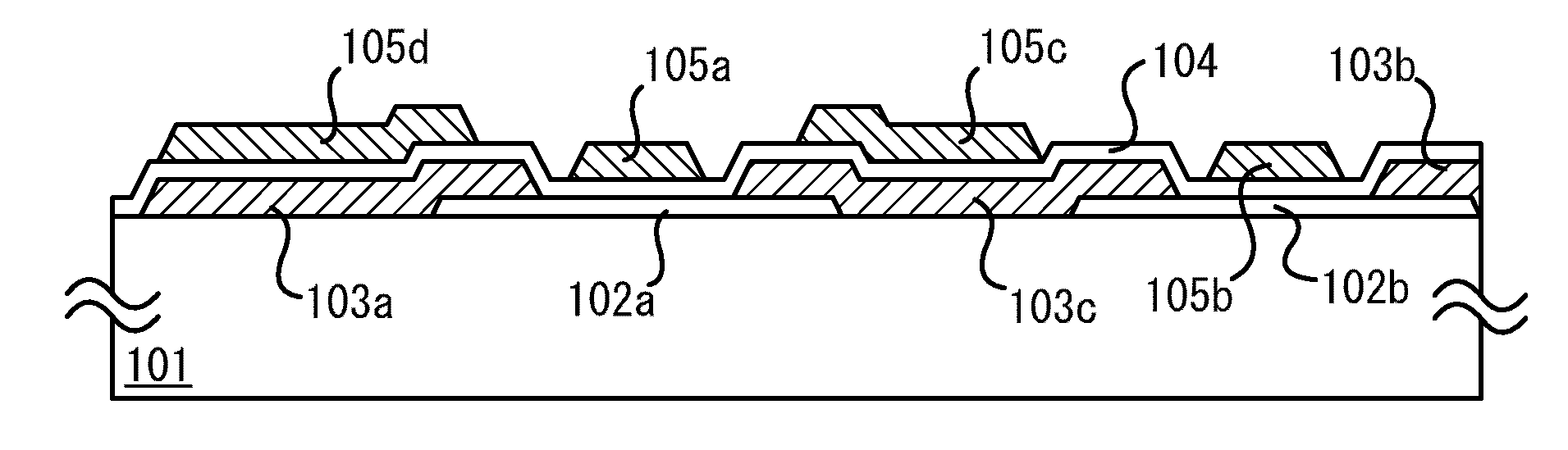
[0081]FIG. 1A is a cross-sectional view of a semiconductor device of this embodiment. The semiconductor device includes a first oxide semiconductor layer 102a and a second oxide semiconductor layer 102b over a substrate 101. Further, a first layer wiring 103a is provided in contact with the first oxide semiconductor layer 102a, a first layer wiring 103b is provided in contact with the second oxide semiconductor layer 102b, and a first layer wiring 103c is provided in contact with the first oxide semiconductor layer 102a and the second oxide semiconductor layer 102b.

[0082]A gate insulator 104 is provided over the first oxide semiconductor layer 102a, the second oxide semiconductor layer 102b, and the first layer wirings 103a to 103c. A second layer wiring 105a, a second layer wiring 105b, a second layer wiring 105c, and a second layer wiring 105d are provided over the gate insulator 104.

[0083]The semiconductor device includes two transistors and two capacitors. The secon...

Example

Embodiment 2

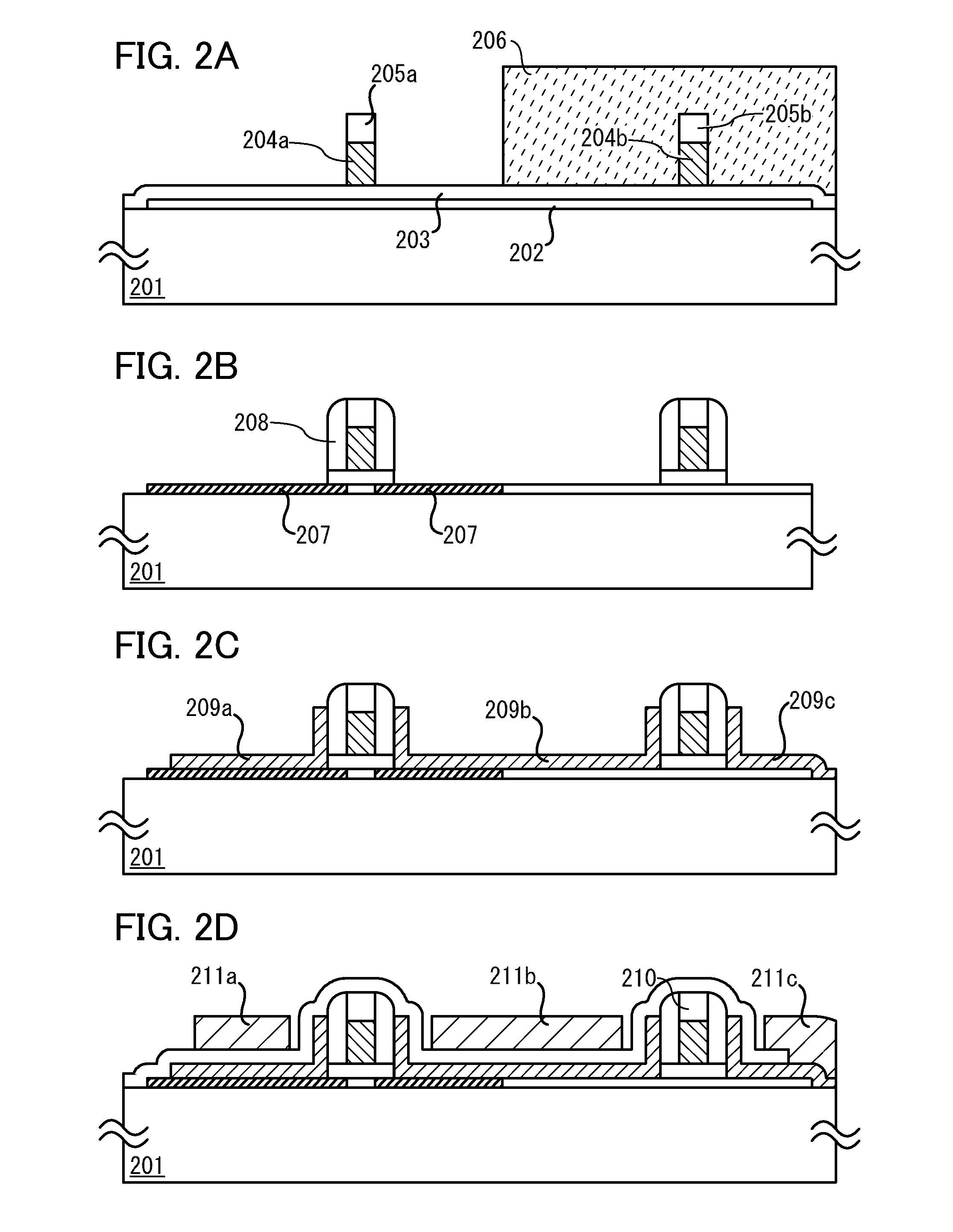
[0089]In this embodiment, a method for manufacturing an offset transistor and an aligned transistor over one oxide semiconductor layer will be described with reference to FIGS. 2A to 2D.

2A>

[0090]An oxide semiconductor layer 202 is formed over a substrate 201. A variety of substrates can be used as the substrate 201. For example, a single crystal silicon wafer, a glass substrate, a silicon on insulator (SOI) substrate, or the like can be used. The substrate 201 preferably has an insulating surface, and in the case where a semiconductor substrate or a conductive substrate is used, an insulating layer (hereinafter, referred to as a first insulating layer) is preferably provided on its surface. A circuit may be formed over the substrate 201, and the first insulating layer may be provided over the circuit.

[0091]The first insulating layer is preferably formed using an oxide, and it is much preferable that the first insulating layer include excessive oxygen. The hydrogen concen...

Example

Embodiment 3

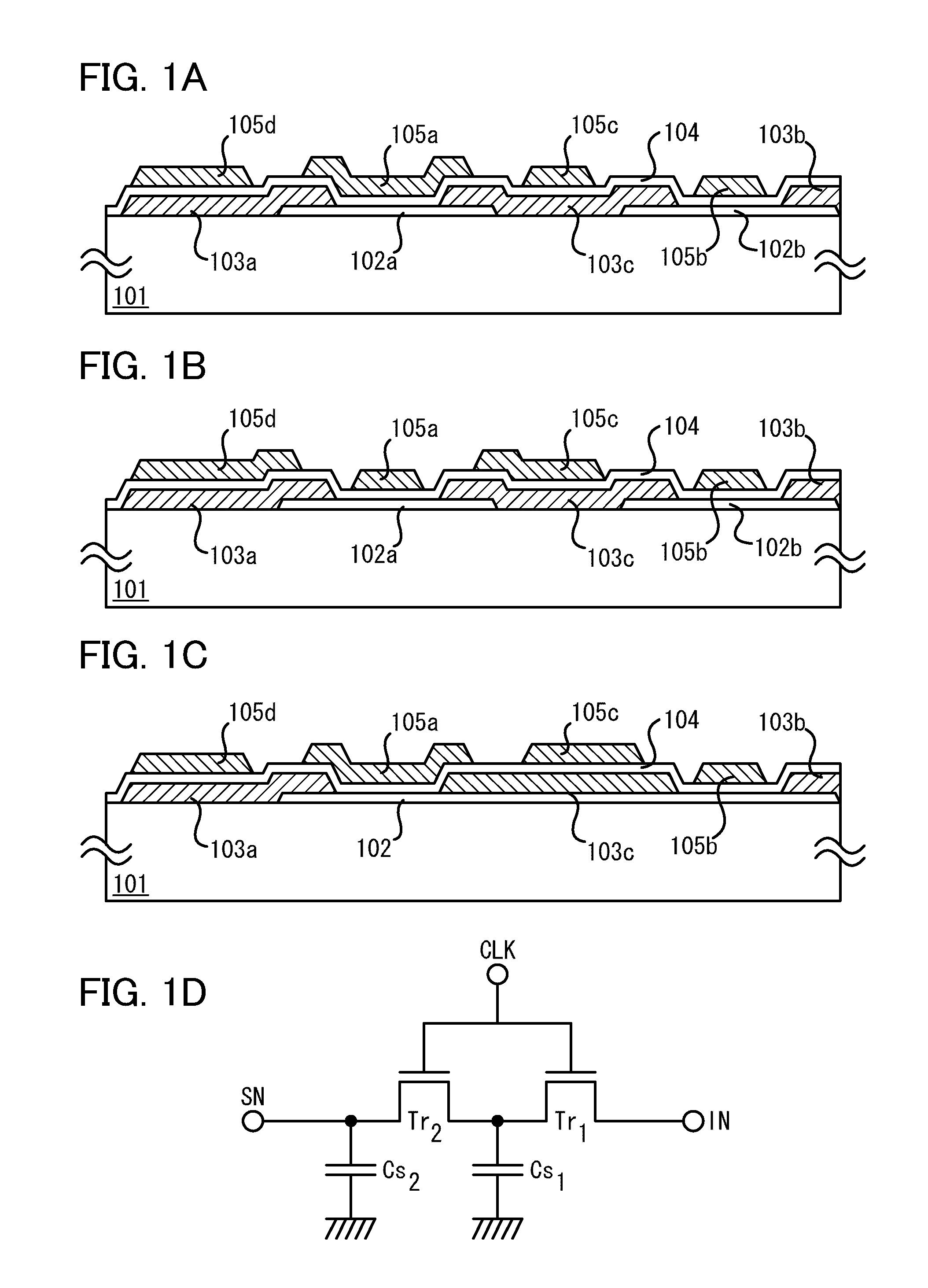
[0112]In this embodiment, an example where the circuit in FIG. 1D is used will be described. FIG. 3A illustrates a circuit of a memory element including the circuit in FIG. 1D. This memory element includes a circuit including a first transistor 301, a second transistor 302, a first capacitor 304, and a second capacitor 305 (a portion surrounded by a dotted line in the drawing) and a read transistor 303. The portion surrounded by the dotted line in the drawing is similar to the circuit in FIG. 1D.

[0113]The first transistor 301 is an offset transistor, and the second transistor 302 is any of an aligned transistor, an overlap transistor, and an offset transistor. Each of the first transistor 301 and the second transistor 302 includes an oxide semiconductor layer as described in Embodiment 1 or 2.

[0114]When data is input, a potential of a signal terminal CLK of gates of the first transistor 301 and the second transistor 302 is controlled so that the first transistor 301 and ...


PUM


Abstract

An offset transistor and a non-offset transistor each including an oxide semiconductor are formed over one substrate. An oxide semiconductor layer, a gate insulator, and first layer wirings which serve as gate wirings are formed. After that, the offset transistor is covered with a resist and impurities are mixed into the oxide semiconductor layer, so that an n-type oxide semiconductor region is formed. Then, second layer wirings are formed. Through the above steps, the offset transistor and the non-offset transistor (e.g., aligned transistor) can be formed.

Description

BACKGROUND OF THE INVENTION[0001]1. Field of the Invention[0002]The present invention relates to a semiconductor including an oxide semiconductor. Note that here, semiconductor devices refer to general elements and devices which function utilizing semiconductor characteristics. For example, a memory, an arithmetic circuit, a rectifier, a display device, and the like which include a semiconductor can be given as semiconductor devices; however, the present invention is not limited thereto. For example, Patent Document 1 can be referred to for a memory including a semiconductor.[0003]2. Description of the Related Art[0004]In recent years, a transistor, a display device, a memory, and the like manufactured using a composite oxide of indium, gallium, and zinc have been reported (for example, see Patent Documents 2 to 5).REFERENCE[0005][Patent Document 1] U.S. Pat. No. 7,468,901[0006][Patent Document 2] U.S. Pat. No. 7,674,650[0007][Patent Document 3] United States Patent Application Publ...

Claims


Application Information

Patent Timeline
IPC IPC(8): H01L29/786H01L29/22H01L27/06
CPCH01L27/0688H01L27/1203H01L27/127H01L27/1225H01L27/1244H01L29/41733
Inventor SAKATA, JUNICHIRO
Owner SEMICON ENERGY LAB CO LTD
Why Eureka
Try Eureka