Laser diode using zinc oxide nanorods and manufacturing method thereof

a zinc oxide nanorod and laser diode technology, applied in lasers, semiconductor devices, semiconductor lasers, etc., can solve the problems of limited use of zinc oxide, low uniformity of nanorod lengths, and insufficient use of nanorods in any functional device other than a transparent electrode, etc., to achieve high crystallinity, low defect, and easy uv laser generation

Active Publication Date: 2012-12-13
DONGGUK UNIV IND ACADEMIC COOPERATION FOUND
View PDF2 Cites 19 Cited by
  • Summary
  • Abstract
  • Description
  • Claims
  • Application Information

AI Technical Summary

Benefits of technology

[0011]According to the embodiments of the present disclosure, it is possible to overcome p-type semiconductor doping difficulties of zinc oxide, while maintaining the advantages of nanostructures including low def...

Problems solved by technology

However, such nanorods are not sufficient to be used in any functional device other than a transparent electrode, because they have an excessively small size and low strength.
However, such a process is still problematic in tha...

Method used


Image

  • Laser diode using zinc oxide nanorods and manufacturing method thereof
  • Laser diode using zinc oxide nanorods and manufacturing method thereof
  • Laser diode using zinc oxide nanorods and manufacturing method thereof

Examples


Embodiment Construction

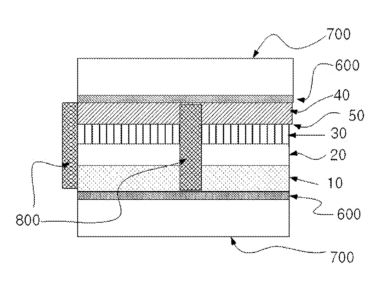
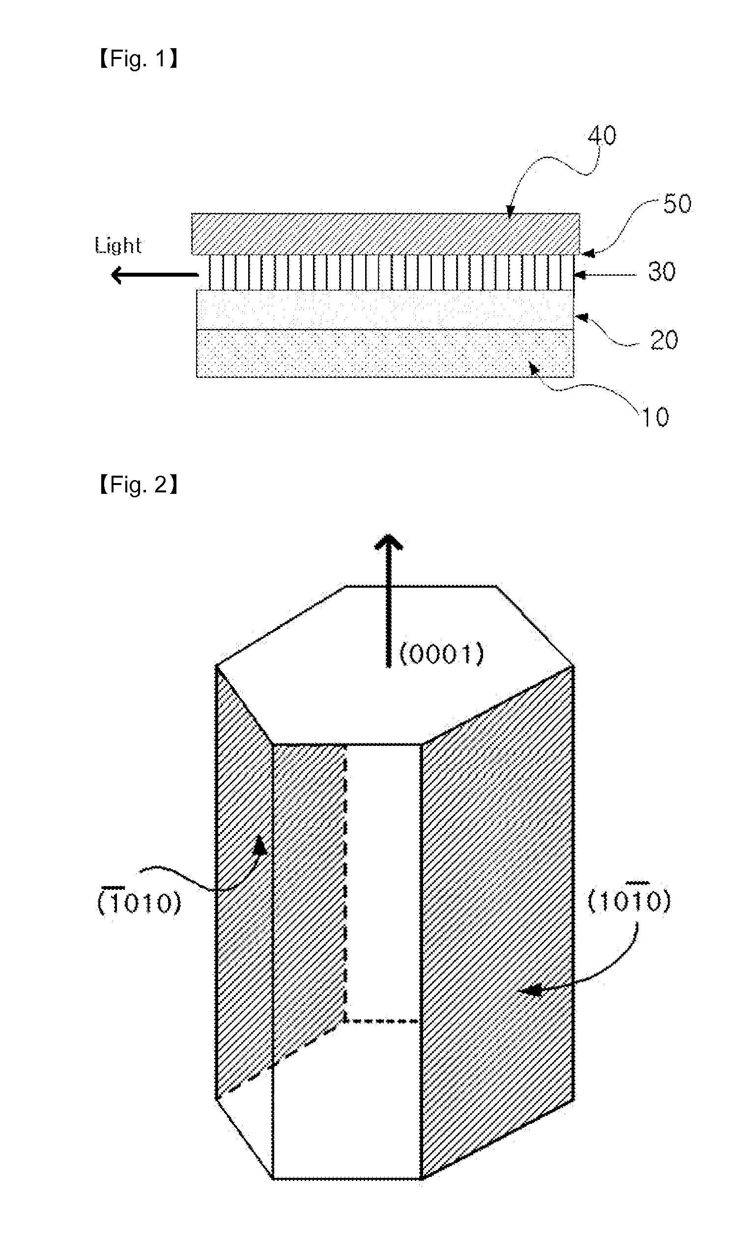
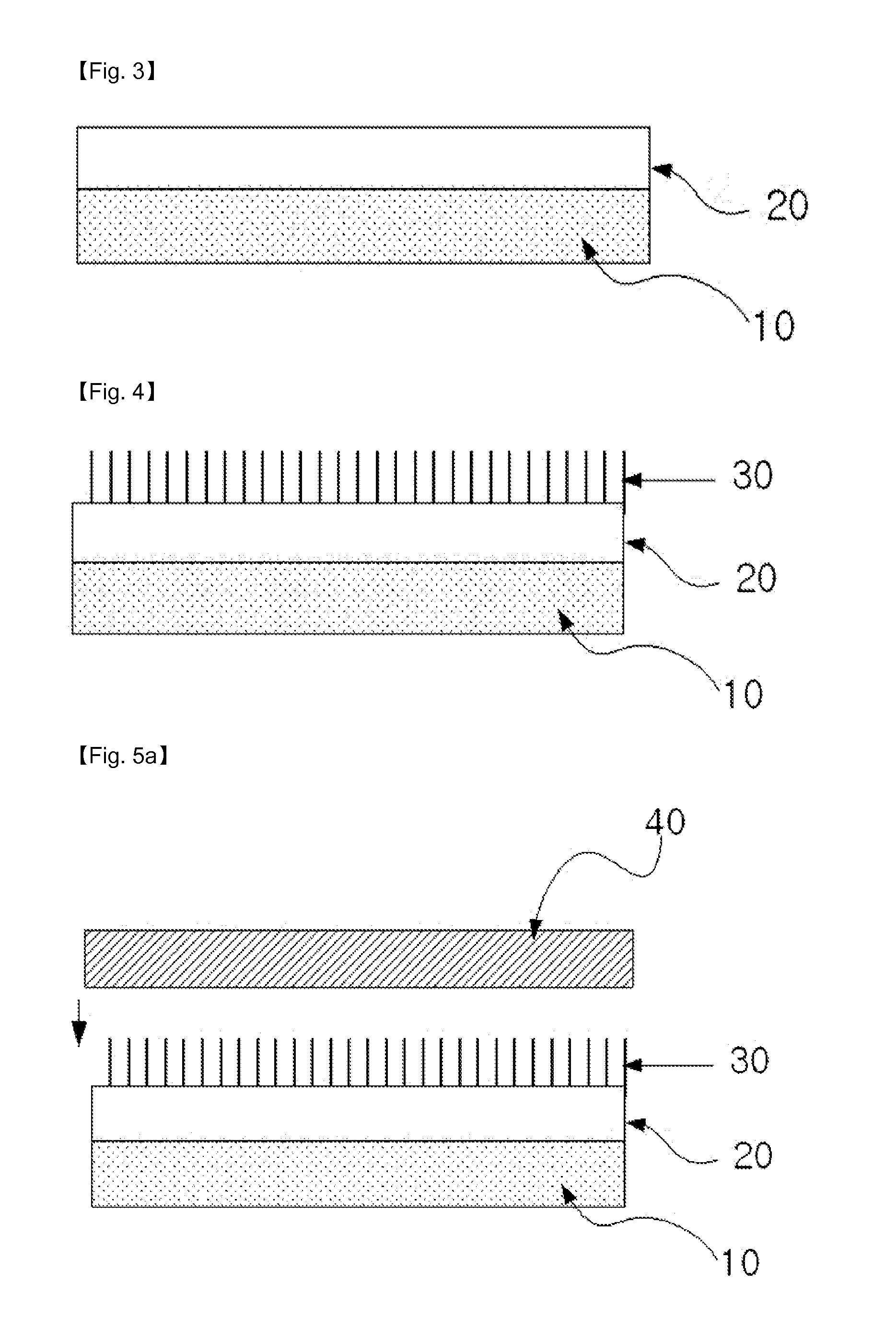
[0018]10: wafer 20: electrode layer[0019]30: n-type zinc oxide nanorod layer[0020]40: p-type single crystal semiconductor layer[0021]50: interface between zinc oxide nanorod layer and single crystal semiconductor layer[0022]600: electrode layer for interconnection[0023]700: heat sink layer[0024]800: epoxy

BEST MODE

[0025]Exemplary embodiments now will be described more fully hereinafter with reference to the accompanying drawings, in which exemplary embodiments are shown. This disclosure may, however, be embodied in many different forms and should not be construed as limited to the exemplary embodiments set forth therein.

[0026]FIG. 1 is a schematic view showing the structure of a laser diode using zinc oxide nanorods according to an embodiment of the present disclosure.

[0027]The laser diode according to an embodiment of the present disclosure uses zinc oxide materials, and is a novel UV (not visible rays) laser diode generating laser through electrical pumping (not optical pumping) in...


PUM


Abstract

Provided are a laser diode using zinc oxide nanorods and a manufacturing method thereof. The laser diode using zinc oxide nanorods according to one embodiment of the present disclosure includes: a wafer; an electrode layer formed on the wafer; a nanorod layer including a plurality of n-doped zinc oxide nanorods grown on the electrode layer; and a p-doped single crystal semiconductor layer that is physically in contact with the ends of the zinc oxide nanorods.

Description

TECHNICAL FIELD[0001]The present disclosure relates to a laser diode emitting ultraviolet rays. More particularly, the present disclosure relates to a laser diode using zinc oxide nanorods and a method for fabricating the same.BACKGROUND ART[0002]Among different nanostructures, one-dimensional structures having a large aspect ratio are called nanowires or nanorods, and synthesis thereof using various materials has been developed significantly. Particular examples of such nanostructures include carbon nanotubes (CNT), cobalt silicide (CoSi), etc. Particularly, it is known that nanostructures grown in the form of nanorods have the advantages of higher crystallinity and lower potential density as compared to those grown in the form of thin films. Carbon nanotube powder has already been developed commercially as a transparent electrode or a negative electrode part for electric field emission.[0003]However, such nanorods are not sufficient to be used in any functional device other than a...

Claims


Application Information

Patent Timeline
IPC IPC(8): H01S5/32H01L33/26B82Y20/00B82Y40/00
CPCB82Y20/00H01S5/021H01S5/341H01S5/327H01S5/0425H01S5/04253H01S5/30
Inventor LEE, SANG WUKKANG, TAE WONPANIN, GENNADYCHO, HAK DONG
Owner DONGGUK UNIV IND ACADEMIC COOPERATION FOUND
Why Eureka
Try Eureka