Thin film and compound used in the same

a technology of thin film and compound, applied in the field of thin film, can solve the problem of high price of iridium, and achieve the effects of low toxicity, small burden on the environment, and excellent light-emitting characteristics

Inactive Publication Date: 2013-01-03
SUMITOMO CHEM CO LTD +2
View PDF0 Cites 9 Cited by
  • Summary
  • Abstract
  • Description
  • Claims
  • Application Information

AI Technical Summary

Benefits of technology

[0008]According to the present invention, the material contains bismuth having the heaviest isotope capable of stably existing among the elements on the Periodic Table, so that there can be provided a material excellent in a light-emitting characteristic for emitting a phosphorescence by the heavy atom effect of bismuth. Although bismuth is a heavy metal, bismuth has low toxicity, so that bismuth can provide a material applying a small amount of burden on the environment. According to the present invention, a bismuth compound having a high solubility in an organic solvent can be provided and a thin film forming composition capable of being easily applied homogeneously is provided. Using the thin film forming composition of the present invention, a thin film having a uniform thickness can be easily formed. The thin film of the present invention can be formed as a thin film causing a small amount of light emission unevenness on the film surface and generating uniform light emission. Furthermore, by using the thin film of the present invention, an element excellent in a light-emitting characteristic can be obtained.

Problems solved by technology

However, iridium exists in an extremely small amount as a resource in the earth's crust, so that the exhaustion of iridium as the resource is feared, and in addition, iridium is expensive.

Method used


Image

  • Thin film and compound used in the same
  • Thin film and compound used in the same
  • Thin film and compound used in the same

Examples


synthesis example 1

Synthesis of 1-phenyl-3,6-bis(trimethylsilyl)dithienobismole

[0225]

[0226]The above synthetic reaction was effected according to the following procedure to synthesize 1-phenyl-3,6-bis(trimethylsilyl)dithienobismole. In the formula, TMS is a trimethylsilyl group.

[0227]Into a 30 mL two-neck flask equipped with a reflux condenser, 0.446 g (0.952 mmol) of 4,4′-dibromo-2,2′-bis(trimethylsilyl)bithiophene and 10 mL of ether were charged and the resultant reaction mixture was cooled down to −80° C. Thereto, 1.25 mL (1.59 M hexane solution, 1.98 mmol) of n-butyl lithium was added and the temperature of the resultant reaction mixture was returned gradually to room temperature, followed by stirring the reaction mixture for around 1 hour. About 0.2 mL of the reaction mixture was sampled and the sample was hydrolyzed, followed by subjecting the hydrolyzed sample to GC (gas chromatography) to confirm the generation of a dilithiated body. On the other hand, into a 30 mL two-neck flask equipped with...

synthesis example 2

Synthesis of 1-phenyl-2,7-dimethyl-3,6-bis(trimethylsilyl)dithienobismole

[0231]

[0232]The above synthetic reaction was effected according to the following procedure to synthesize 1-phenyl-2,7-dimethyl-3,6-bis(trimethylsilyl)dithienobismole.

[0233]Into a 10 mL two-neck flask, 0.468 g (1 mmol) of 4,4′-dibromo-3,3′-dimethyl-2,2′-bis(trimethylsilyl)bithiophene and 5 mL of ether were charged and the resultant reaction mixture was cooled down to −80° C. Thereto, 1.27 mL (1.56 M hexane solution, 2 mmol) of n-butyl lithium was added and the temperature of the resultant reaction mixture was returned gradually to room temperature, followed by stirring the reaction mixture for around 1 hour. About 0.2 mL of the reaction mixture was sampled and the sample was hydrolyzed, followed by subjecting the hydrolyzed sample to GC to confirm the generation of a dilithiated body. On the other hand, into a 20 mL Schlenk tube equipped with a dropping funnel, 5 mL of THF and 0.540 g (1 mmol) of diiodophenyl bi...

synthesis example 3

Synthesis of 1-phenyl-2,4-di(benzo[b]thieno)bismole

[0237]

[0238]The above synthetic reaction was effected according to the following procedure to synthesize 1-phenyl-2,4-di(benzo[b]thieno)bismole.

[0239]Into a 20 mL Schlenk tube, 0.424 g (1.00 mmol) of 3,3′-dibromo-2,2′-bi(benzo[b]thiophene) and 5 mL of ether were charged and the resultant reaction mixture was cooled down to −80° C. Thereto, 1.27 mL (1.56 M hexane solution, 2.00 mmol) of n-butyl lithium was added and the temperature of the resultant reaction mixture was returned gradually to room temperature, followed by stirring the reaction mixture for around 1 hour. By GC, the generation of a dilithiated body was confirmed. Thereinto, 0.540 g (1.00 mmol) of diiodophenyl bismuth dissolved in 5 mL of THF was dropped at 0° C. and the resultant reaction mixture maintained at 0° C. was stirred over one night. By TLC, the disappearance of the substrate was confirmed. From the reaction mixture, the solvent was distilled off by an evaporat...


PUM

PropertyMeasurementUnit
thicknessaaaaaaaaaa
triplet excitation energyaaaaaaaaaa
compositionaaaaaaaaaa

Abstract

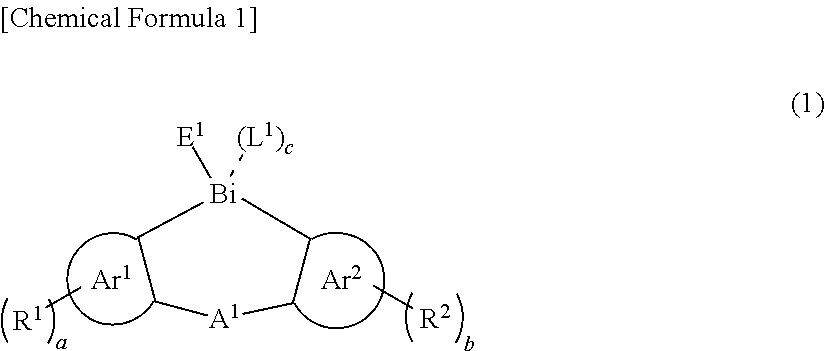
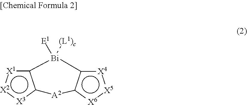
To provide a novel material exhibiting excellent light-emitting characteristics using a heavy metal element having relatively abundant reserve.A thin film containing a compound of Formula (1):wherein Ar1 and Ar2 are each independently a C3-30 aromatic ring; R1 and R2 are a substituent; a and b are each independently an integer of 0 to 12, wherein when a is 2 or more, each R1 is optionally different from each other and two R1 are optionally bonded with each other to form a ring structure, and when b is 2 or more, each R2 is optionally different from each other and two R2 are optionally bonded with each other to form a ring structure; A1 is any of direct bond, —O—, —S—, —S(═O)—, —S(═O)2—, —PR3—, —NR4—, and —C(—R5)2—; R3 is a hydrogen atom or a substituent; R4 is a hydrogen atom or a substituent; R5 is a hydrogen atom or a substituent and two R5 are optionally different from each other; E1 is a monovalent group having 50 or less carbon atoms; L1 is a ligand having 50 or less carbon atoms; c is an integer of 0 to 3, wherein when c is 2 or more, each L1 is optionally different from each other; and each combination of a combination of E1 and Ar1 and a combination of E1 and Ar2 optionally forms a bond; and when c is 1 to 3, each combination of a combination of L1 and E1, a combination of L1 and Ar1, a combination of L1 and Ar2, and a combination of L1 and L1 optionally forms a bond.

Description

TECHNICAL FIELD[0001]The present invention relates to a thin film comprising an organic compound containing bismuth in the structural skeleton thereof, a coating liquid for forming the thin film, an element comprising the thin film, and a novel compound capable of being used in the thin film.BACKGROUND ART[0002]One of the characteristics of an electronic device and an optical device using an organic compound is such a point in that, by forming a thin film controlled in a nano-scale by a method for forming the film in a solution state, a device making the most of the characteristics of the organic compound can be produced. In a device such as an organic electric field electroluminescent device (hereinafter, also called as organic EL element), an organic solar cell, and an organic transistor, which are an electronic device or an optical device of which development has been activated in recent years, such a thin film controlled in a nano-scale or a layered structure of the thin film is...

Claims


Application Information

Patent Timeline
Patent Type & Authority Applications(United States)
IPC IPC(8): C07F9/94C09K11/06B82Y30/00
CPCC07F9/94H01L51/0077H01L51/5016H05B33/145C09K2211/188C09K2211/1044C09K2211/1088C09K2211/1092C09K2211/1029H10K85/30H10K50/11H10K2101/10
Inventor OHSHITA, JOJIMURAFUJI, TOSHIHIROKURAMOCHI, YUSUKEKAIKOH, TAKASHIHIGASHIMURA, HIDEYUKI
Owner SUMITOMO CHEM CO LTD
Why Eureka
Try Eureka