

Particle-Based Precursor Formation Method and Photovoltaic Device Thereof
a precursor and particle technology, applied in semiconductor devices, coatings, inks, etc., can solve the problems of reducing the efficiency of the device, reducing the number of components, and reducing the risk of ignition, so as to reduce the need for enhancing organic additives, reduce production costs and complexity, and avoid or reduce the necessity of enhancing organic additives.
- Summary
- Abstract
- Description
- Claims
- Application Information
AI Technical Summary
Benefits of technology
Problems solved by technology
Method used
Image

Examples
example 1
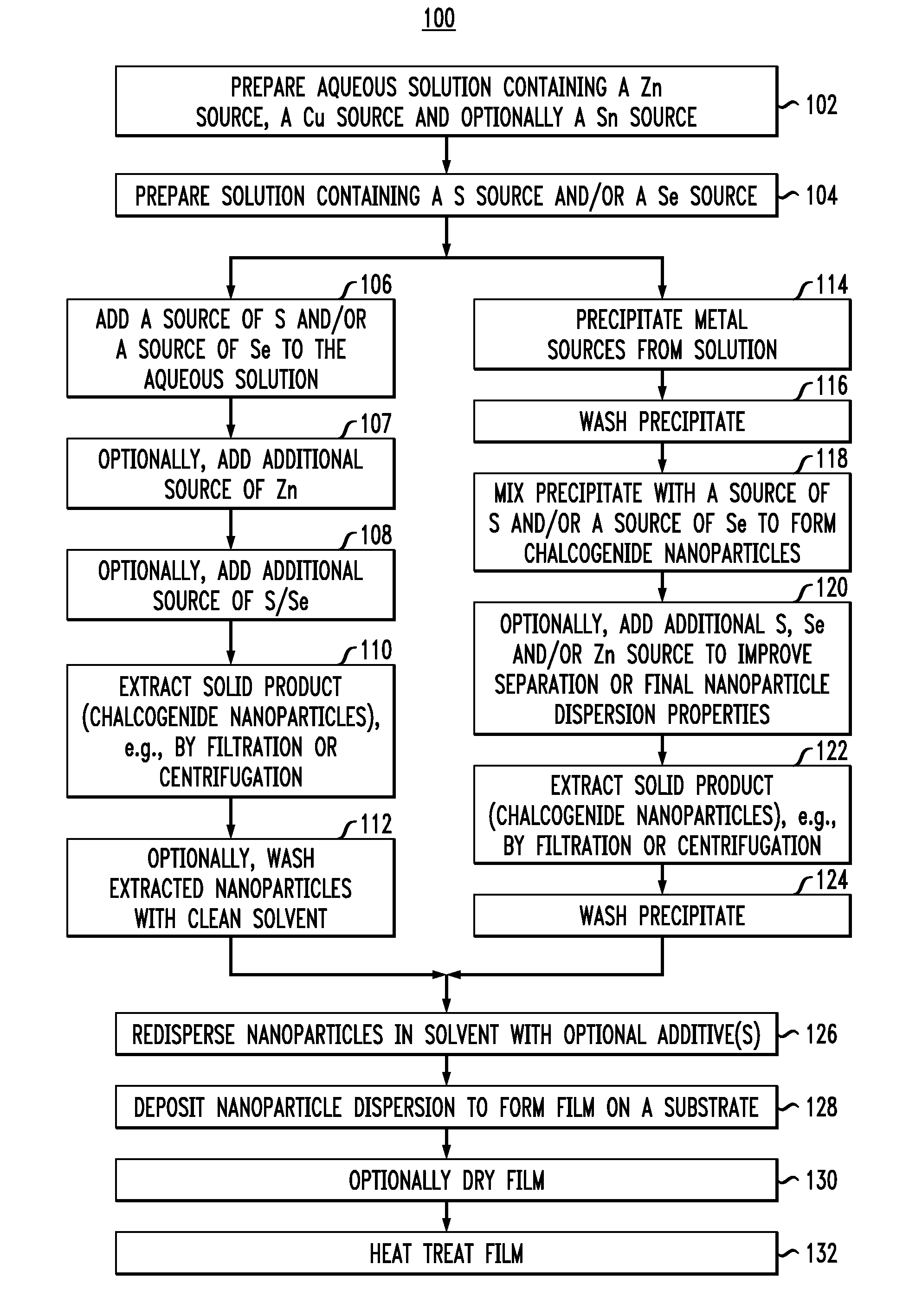
[0063]Particle dispersion preparation: zinc chloride (ZnCl2) (0.067 grams (g)), copper chloride (CuCl2) (0.967 g), and tin chloride (SnCl2) (0.765 g) were dissolved in 30 milliliters (ml) of water (full dissolution can be achieved by addition of HCl, but in this example this was not targeted and the mixture had a white opaque aspect due to partial hydroxide formation). Under stirring, 5 ml 12 percent (%) (approx.) ammonium selenide solution was added, followed by addition of a solution of ZnCl2 (0.600 g) in 10 ml water and finally 5 ml 20% ammonium sulfide solution. The solution was sonicated for 10 minutes, stirred again and separated by two consecutive cycles of centrifugation and washing with from about 2% to about 3% aqueous ammonium sulfide. The final wet cake was dispersed with the addition of water to form dispersion A with a total volume of 12 ml.
example 1.1
[0064]Coating ink preparation: Coating ink B was prepared by mixing 3 ml of dispersion A, 1 ml of water and Solution C containing 1.5 ml hydrazine, 1.2 ml water, 0.23 g Se, 0.05 g SnS.
example 1.2
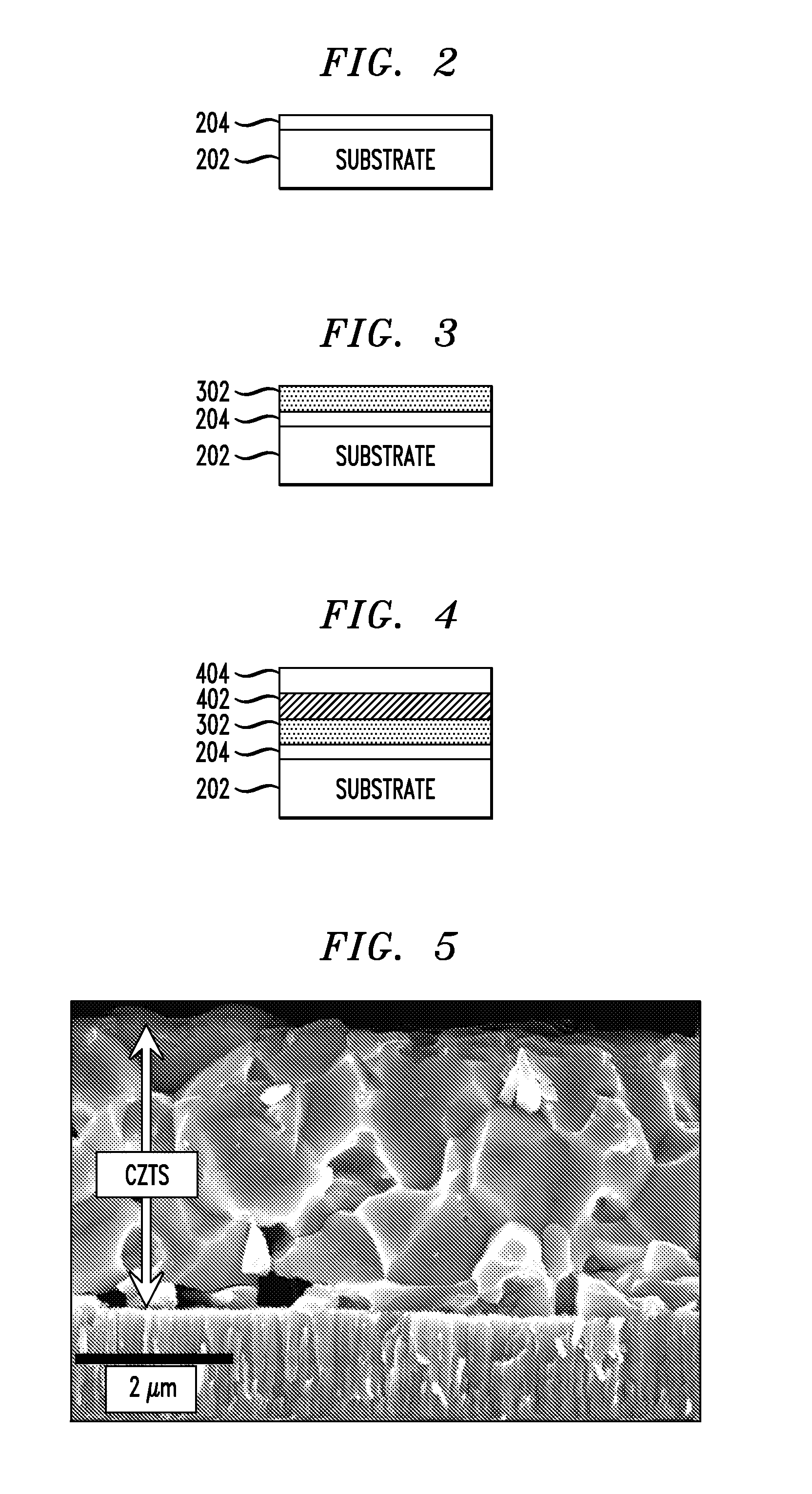
[0065]Film deposition: One layer of the ink was spin-coated at 500 revolutions per minute (rpm) followed by 5 layers at 250 rpm. Each layer was annealed at 425° C. before the next layer was deposited. Solution D, containing 1 g Se and 0.05 g SnS in 4.5 ml 33% aqueous hydrazine, was coated on top at 800 rpm and the sample was annealed on a hot plate preset at 600° C. for 10 minutes. An image of the film prepared is provided in FIG. 5. As demonstrates in FIG. 5, kesterite grains larger than 1 micrometer in at least one dimension can readily be achieved using this technique. The use of capping layers in the fabrication of kesterite films is described in U.S. patent application Ser. No. ______, filed herewith on the same day of ______, entitled “Capping Layers for Improved Crystallization,” designated as Attorney Reference Number YOR920110408US1, the entire contents of which are incorporated by reference herein.
PUM
 Abstract
Description
Claims
Application Information