Laser annealing for thin film solar cells

a solar cell and film technology, applied in the field of thin film solar cell processing, can solve the problems of low absorption coefficient of crystalline silicon, increased cost of crystalline silicon solar cell technology, and reduced manufacturing cost, so as to improve the efficiency of solar cell, increase the density, and increase the grain size

Inactive Publication Date: 2013-03-14
INTERMOLECULAR
View PDF15 Cites 17 Cited by
  • Summary
  • Abstract
  • Description
  • Claims
  • Application Information

AI Technical Summary

Benefits of technology

[0012]In some embodiments of the present invention, CIGS, CZTS, or CdTe films are printed on a substrate followed by an anneal using a laser. The laser anneal may result in a film with higher density and larger grains.
[0013]In some embodiments of the present invention, a Na-free CIGS layer is followed by the deposition of Na2Se. This film stack is then annealed using a laser to incorporate the Na into the underlying CIGS layer in a uniform manner and improve the efficiency of the solar cell.
[0014]In some embodiments of the present invention, a laser is used to ablate oxides and excess Na from the surface of a CIGS absorber layer in an inert atmosphere. In some embodiments of the present invention, a laser is used to ablate oxides from the surface of a CZTS absorber layer in an inert atmosphere. The substrate can then be transported into a dry deposition chamber f

Problems solved by technology

Also, the absorption coefficient is low for crystalline silicon because of the indirect band gap.
Therefore, crystalline silicon solar cell technologies lead to increased costs.
Additionally, thin film solar cells can be fabricated at the module level, thus further decreasing the manufacturing costs.
However, the supply of In, Ga and Te may impact annual production of CIGS and CdTe solar panels.
Moreover, price increases and supply constraints in In and Ga could result from the aggregate demand for these materials used in flat panel displays (FPD) and light-emitting diodes (LED) along with CIGS TFPV.
Also, there are concerns about the toxicity of Cd throughout the lifecycle o

Method used


Image

  • Laser annealing for thin film solar cells
  • Laser annealing for thin film solar cells
  • Laser annealing for thin film solar cells

Examples


Embodiment Construction

[0026]A detailed description of one or more embodiments is provided below along with accompanying figures. The detailed description is provided in connection with such embodiments, but is not limited to any particular example. The scope is limited only by the claims and numerous alternatives, modifications, and equivalents are encompassed. Numerous specific details are set forth in the following description in order to provide a thorough understanding. These details are provided for the purpose of example and the described techniques may be practiced according to the claims without some or all of these specific details. For the purpose of clarity, technical material that is known in the technical fields related to the embodiments has not been described in detail to avoid unnecessarily obscuring the description.

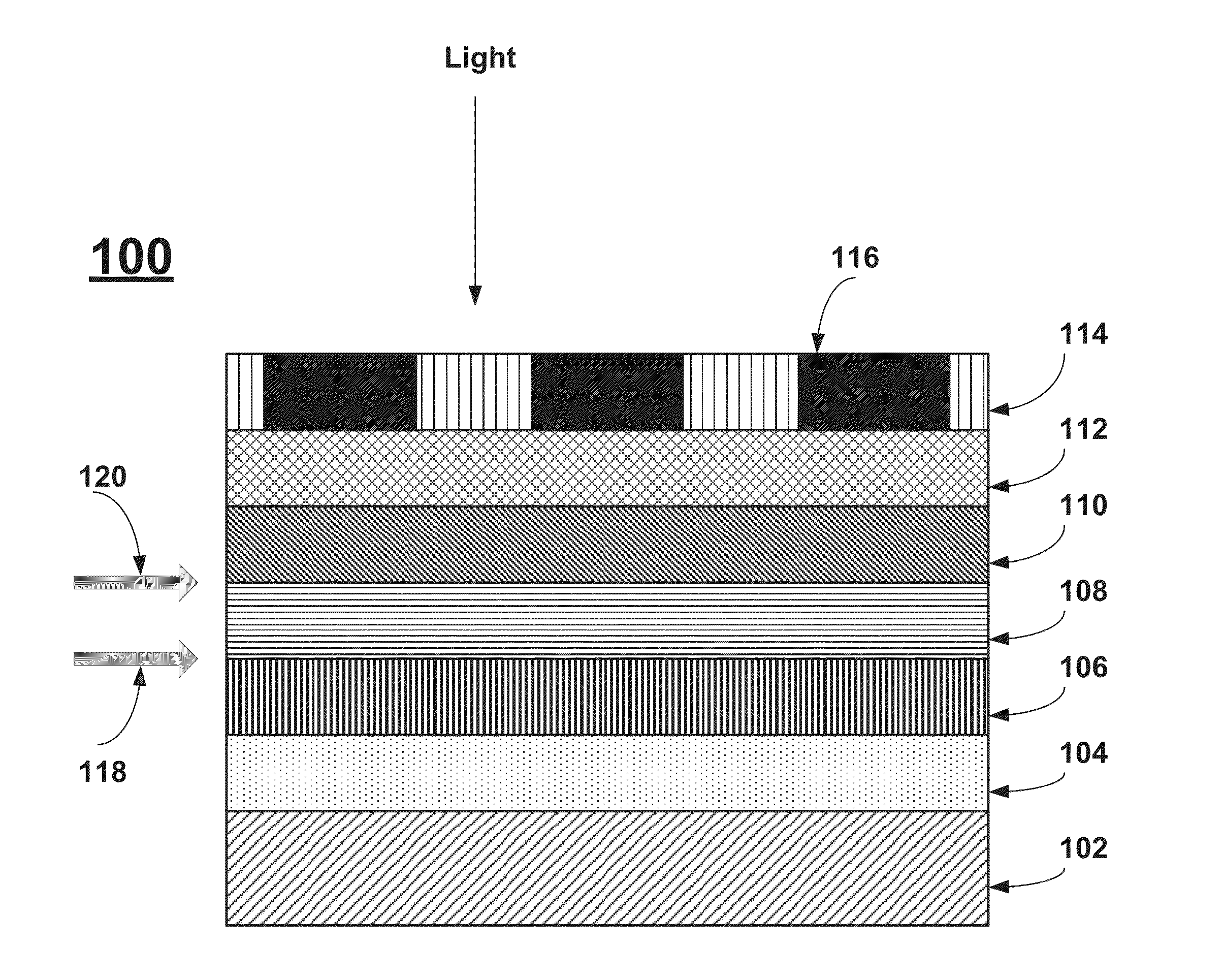
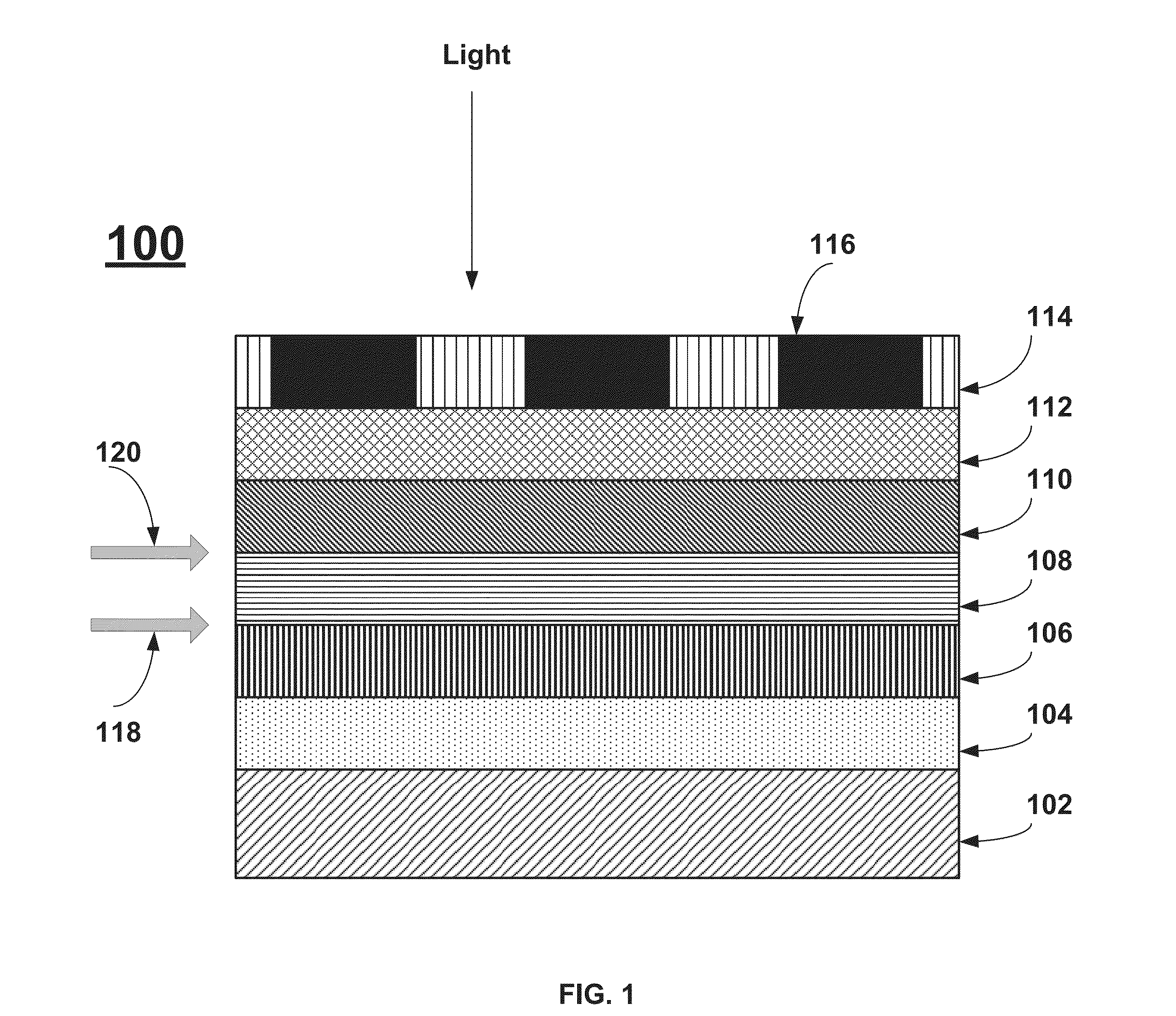
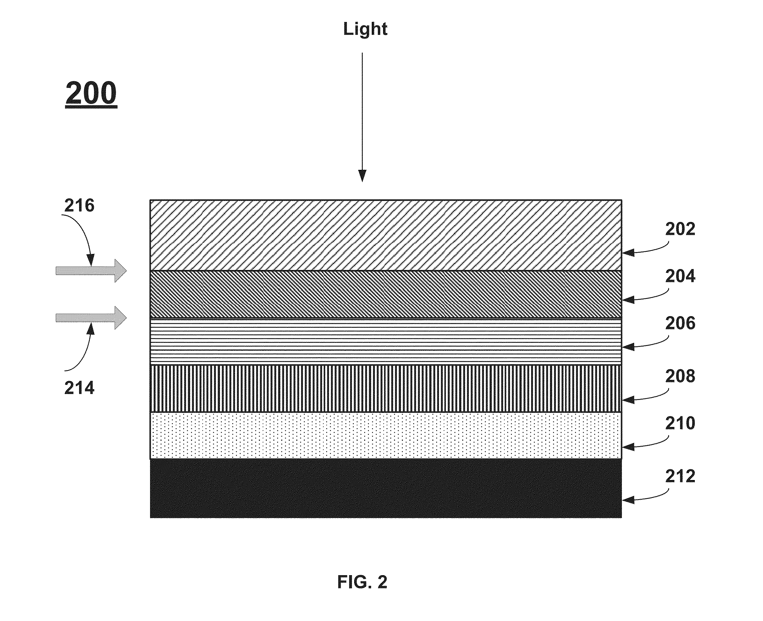
[0027]As used herein, “CIGS” will be understood to represent the entire range of related alloys denoted by Cu(InxGa1-x)(SySe2-y) where 0≦x≦1 and 0≦y≦2. As used herein, “CZTS” ...


PUM


Abstract

A method for forming copper indium gallium (sulfide) selenide (CIGS) solar cells, cadmium telluride (CdTe) solar cells, and copper zinc tin (sulfide) selenide (CZTS) solar cells using laser annealing techniques to anneal the absorber and/or the buffer layers. Laser annealing may result in better crystallinity, lower surface roughness, larger grain size, better compositional homogeneity, a decrease in recombination centers, and increased densification. Additionally, laser annealing may result in the formation of non-equilibrium phases with beneficial results.

Description

FIELD OF THE INVENTION[0001]The present invention relates generally to thin film solar cell processing. More specifically, this invention relates to methods of forming copper indium gallium (sulfide) selenide (CIGS) solar cells, cadmium telluride (CdTe) solar cells, and copper zinc tin (sulfide) selenide (CZTS) solar cells using laser annealing techniques.BACKGROUND OF THE INVENTION[0002]Solar cells have been developed as clean, renewable energy sources to meet growing demand. Currently, crystalline silicon solar cells (both single crystal and polycrystalline) are the dominant technologies in the market. Crystalline silicon solar cells must use a thick substrate (>100 um) of silicon to absorb the sunlight since it has an indirect band gap. Also, the absorption coefficient is low for crystalline silicon because of the indirect band gap. The use of a thick substrate also means that the crystalline silicon solar cells must use high quality material to provide long minority carrier l...

Claims


Application Information

Patent Timeline
IPC IPC(8): H01L31/0264
CPCH01L31/0749Y02E10/541H01L31/1864H01L31/0326H01L31/0322Y02P70/50
Inventor LIANG, HAIFANDUREN, JEROEN VANSUN, ZHI-WEN
Owner INTERMOLECULAR
Why Eureka
Try Eureka