Photocatalyst material and photocatalyst device

a photocatalyst and material technology, applied in the field of photocatalyst materials and photocatalyst devices, can solve the problems of low hydrogen generation efficiency, poor sunlight use efficiency, and material itself moltenness, and achieve the effects of enhancing photocatalyst efficiency and hydrogen generation efficiency, and reducing the number of molten materials

Inactive Publication Date: 2013-05-02
SAKAI CHEM IND CO LTD +1
View PDF1 Cites 17 Cited by
  • Summary
  • Abstract
  • Description
  • Claims
  • Application Information

AI Technical Summary

Benefits of technology

[0033]The photocatalyst material of the present invention has an intermediate band formed of an impurity band between band gaps, and thus, the photocatalyst material can absorb light in the visible ray region and the infrared ray region, which cannot be absorbed by a parent material before replacement of a 3d-transition metal, as well as in an ultraviolet ray region. That is, the photocatalyst material has a light absorption coefficient of 1,000 cm−1 or more in an entire wavelength region of 1,500 nm or less and 300 nm or more. Conventionally, in this wavelength region, a photocatalyst material has a minimum value of a light absorption coefficient of about 600 to 700 cm−1 in GaN and 200 to 300 cm−1 similarly in AlN, whereas the photocatalyst material of the present invention has a very large light absorption coefficient. Thus, it is possible to use sunlight having a wavelength which cannot be used in a parent material before replacement of a 3d-transition metal, and thus, photocatalyst efficiency and hydrogen generation efficiency can be enhanced. Further, the photocatalyst material of the present invention has a large light absorption coefficient with respect to light in a broad wavelength band, and thus, even when a wavelength distribution of sunlight on the earth changes due to a change in weather such as fair, cloudy, and rainy days, a photocatalytic effect with little change can be achieved.
[0034]Further, the photocatalyst material of the present invention is produced at high temperatures of from 300° C. to 1,000° C., and thus, is excellent in stability with respect to heat. The photocatalyst material of the present invention is also ...

Problems solved by technology

Thus, there is a problem in that TiO2 is active only in an ultraviolet ray region with a wavelength of 390 nm or less and has poor use efficiency of sunlight and low hydrogen generation efficiency although TiO2 has a high photocatalytic function.
However, there is a problem in that the material itself is molten by oxidation due to holes generated in the valence band when the material is irradiated with light and does not function stably.
Organic materials have also been sought for, but have not been put into practical use as well due to the serious stability problem o...

Method used


Image

  • Photocatalyst material and photocatalyst device
  • Photocatalyst material and photocatalyst device
  • Photocatalyst material and photocatalyst device

Examples


first embodiment

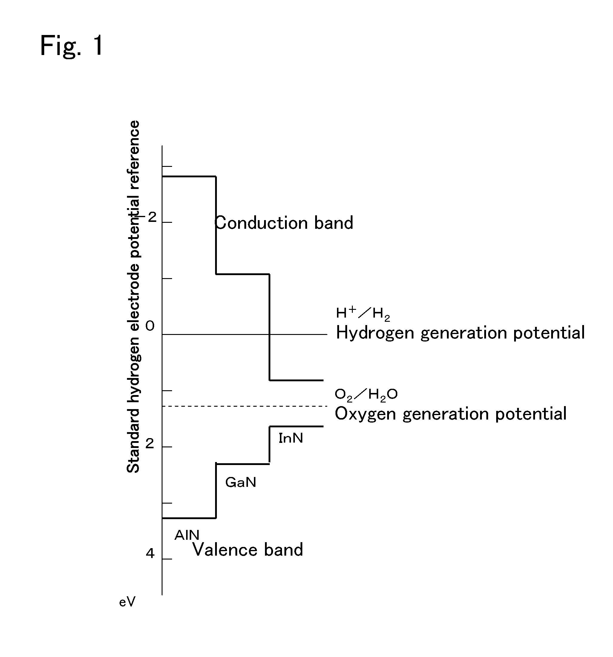
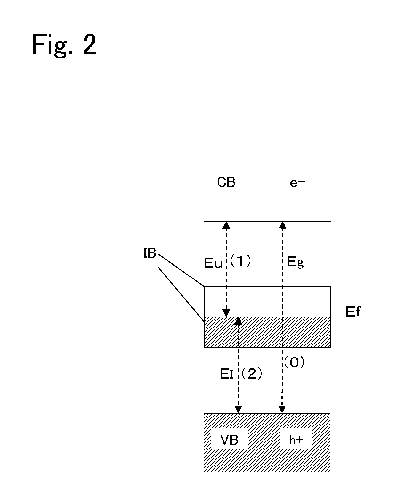
[0091]FIG. 2 is a schematic view illustrating an example of a band structure of GaMnN of the present invention. In FIG. 2, symbol VB denotes a valence band; CB, a conduction band; IB, an intermediate band formed of an impurity band; Eg, a band gap of GaMnN; Ef, a Fermi level; Eg, a band gap between the impurity band and the conduction band; and El, a band gap between the valence band and the impurity band. Here, even when the intermediate band is present, the band gap Eg of GaMnN is the same as a band gap of GaN without Mn added thereto. By radiation of sunlight to GaMnN, three types of excitations occur as follows: electrons e− are directly excited by ultraviolet rays from the valence band VB to the conduction band CB (represented by (0) in FIG. 2); electrons e− are excited by visible rays and infrared rays from the valence band VB to an unoccupied portion of the impurity band IB through the intermediate band IB (represented by (2) in FIG. 2); and electrons e− are excited from the ...

second embodiment

[0096]FIG. 4 is a schematic view illustrating an example of a band structure which is a laminated structure of p-GaN / GaMnN. In FIG. 4, symbol 211 denotes a p-GaN layer; 212, a GaMnN layer; VB, a valence band; CB, a conduction band; IB, an intermediate band formed of an impurity band; Eg, a band gap of GaMnN; Ef, a Fermi level; Eu, a band gap between the impurity band and the conduction band; and El, a band gap between the valence band and the impurity band. FIG. 4 illustrates that, by radiation of light to the GaMnN layer 212, electrons e− are directly excited from the valence band to the conduction band (0); electrons are excited from the valence band to an unoccupied portion of the impurity band through the impurity band (2); and electrons are excited from an occupied portion of the impurity band to the conduction band (1). The excited electrons e− are blocked by the p-GaN layer 211 and stay in the GaMnN layer 212, and the holes h+ move to the p-GaN layer 211, with the result that...

third embodiment

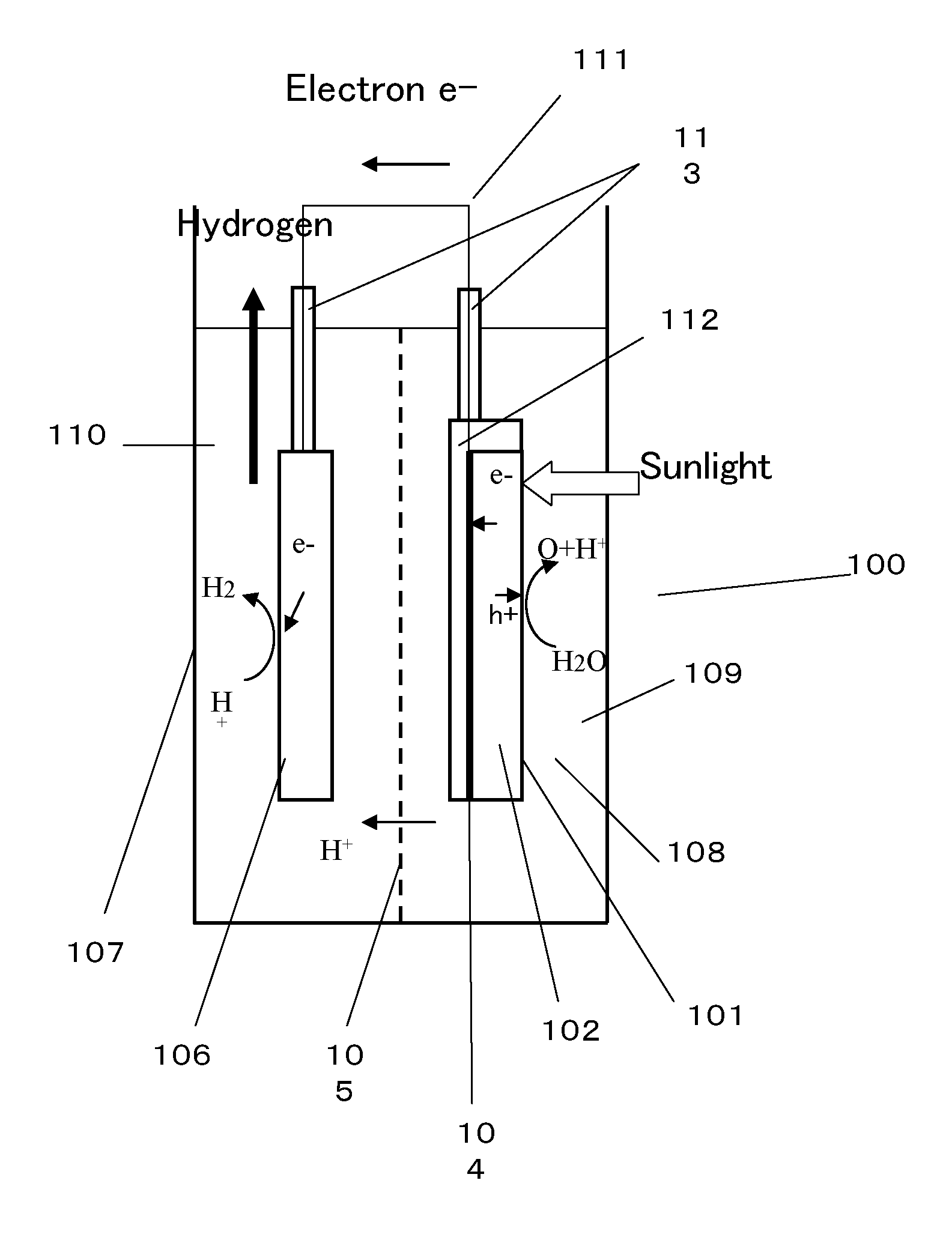
[0099]FIG. 6 is a schematic view illustrating a structure of a photocatalyst device 300 using, as a cathode, the photocatalyst material having the laminated structure of p-GaN / GaMnN illustrated in FIG. 4. A water tank 307 is filled with pure water or an electrolyte aqueous solution 308 and divided into a cathode chamber 309 and an anode chamber 310 by an ion exchange membrane 305. A platinum plate is placed as an anode 306 in the anode chamber 310, and a cathode 301 is placed in the cathode chamber 309. The cathode 301 has a structure in which a GaMnN layer 302 is laminated on one principal surface of a p-GaN layer 303, and a charge extracting electrode 304 is formed on the other principal surface of the p-GaN layer 303. The charge extracting electrode 304 is coated with a waterproof insulating film 312 so as not to come into direct contact with the electrolyte aqueous solution 308. Numeral 313 denotes waterproof insulating tubes for preventing a conductive wire 311 from coming into...


PUM

PropertyMeasurementUnit
Nanoscale particle sizeaaaaaaaaaa
Semiconductor propertiesaaaaaaaaaa

Abstract

A photocatalyst material and a photocatalyst device capable of generating hydrogen from water by radiation of sunlight at high efficiency. The photocatalyst material according to the present invention includes a nitride-based compound semiconductor obtained by replacement of part of Ga and/or Al by a 3d-transition metal. The nitride-based compound semiconductor has one or more impurity bands. A light absorption coefficient of the nitride-based compound semiconductor is 1,000 cm−1 or more in an entire wavelength region of 1,500 nm or less and 300 nm or more. Further, the photocatalyst material satisfies the following conditions: the energy level of the bottom of the conduction band is more negative than the redox potential of H+/H2; the energy level of the top of the valence band is more positive than the redox potential of O2/H2O; and there is no or little degradation of a material even when the material is irradiated with light underwater.

Description

TECHNICAL FIELD[0001]The present invention relates to a photocatalyst material and a photocatalyst device, and more specifically, to a photocatalyst material having a multiband structure capable of performing a photocatalytic operation in infrared, visible, and ultraviolet ray regions and a photocatalyst device using the photocatalyst material.BACKGROUND ART[0002]In recent years, against the backdrop of a global environmental problem such as a CO2 emission problem caused by the use of fossil fuel, and an energy cost problem such as a rise in crude oil price, there has been an increasing expectation toward creation of clean new energy, as typified by a solar cell, a fuel cell and an energy device which use hydrogen as fuel, and the like. Instead of a method of obtaining hydrogen, which is fuel for the fuel cell, the energy device, and the like, from fossil fuel, a method of producing hydrogen from water using a water decomposition photocatalyst has the high potential to contribute to...

Claims


Application Information

Patent Timeline
IPC IPC(8): C25B11/04
CPCB01J27/24B01J35/004C01B13/0207C25B11/0478Y02E60/364C01B3/042C25B1/04C25B1/55C25B11/091Y02E10/542Y02E60/36Y02P70/50H01G9/205
Inventor SONODA, SAKIKAWASAKI, OSAMUKATO, JUNICHITAKENAGA, MUTSUO
Owner SAKAI CHEM IND CO LTD
Why Eureka
Try Eureka