

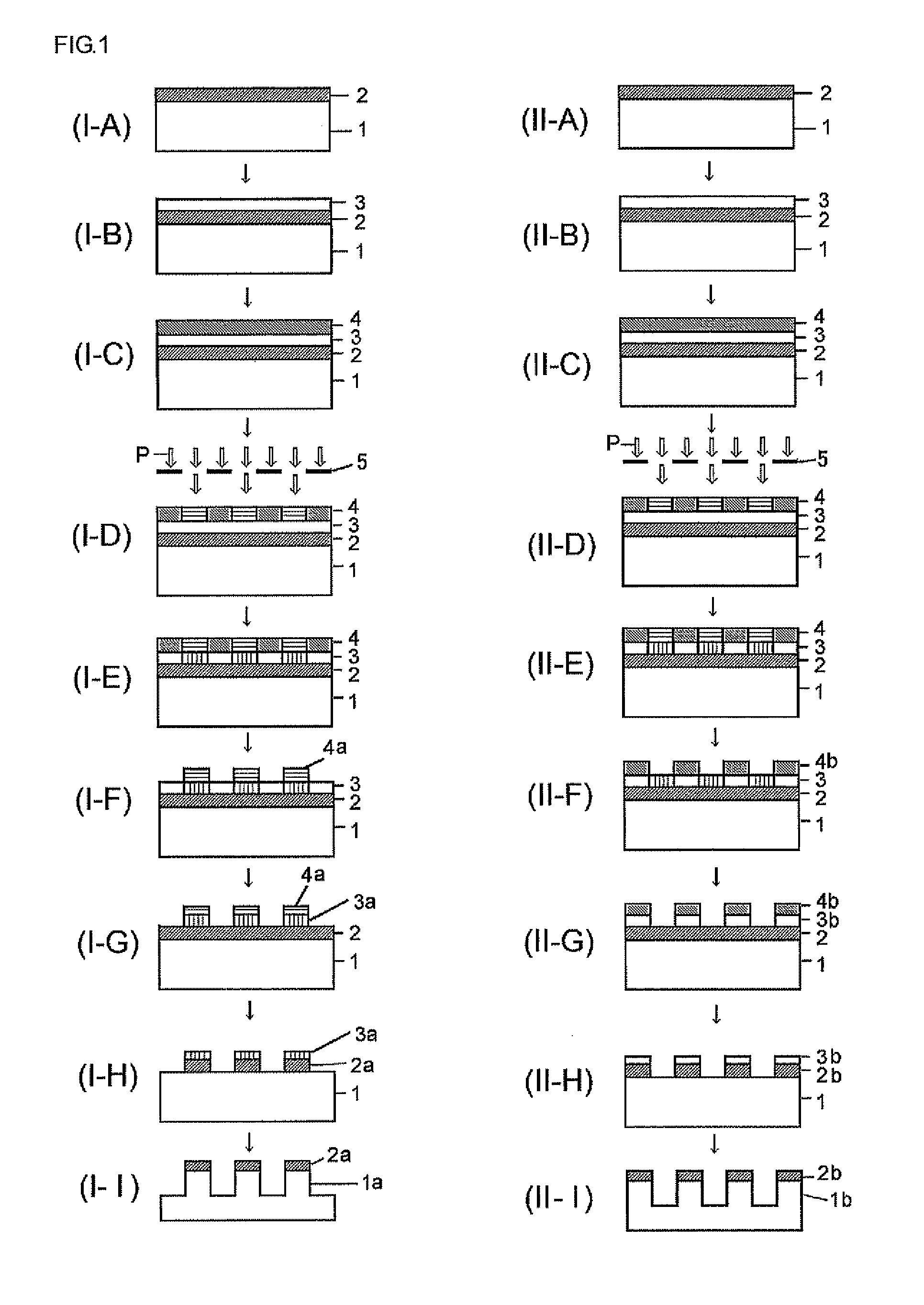
Silicon-containing resist underlayer film-forming composition and patterning process
a technology of film-forming composition and under-layer film, which is applied in the direction of photosensitive materials, instruments, photomechanical equipment, etc., can solve the problems of irrational economic rationality and inability to express under-layer resist satisfactorily, and achieve the effect of high precision
- Summary
- Abstract
- Description
- Claims
- Application Information
AI Technical Summary
Benefits of technology
Problems solved by technology
Method used
Image

Examples
examples
[0195]Although Synthesis Examples, Examples, and Comparative Examples will be shown and the present invention will be explained in detail hereafter, the present invention is not restricted to the following Examples. Note that the symbol “%” in the Examples represents a mass %, and the molecular weight measurement was based on GPC.
synthesis example a-1
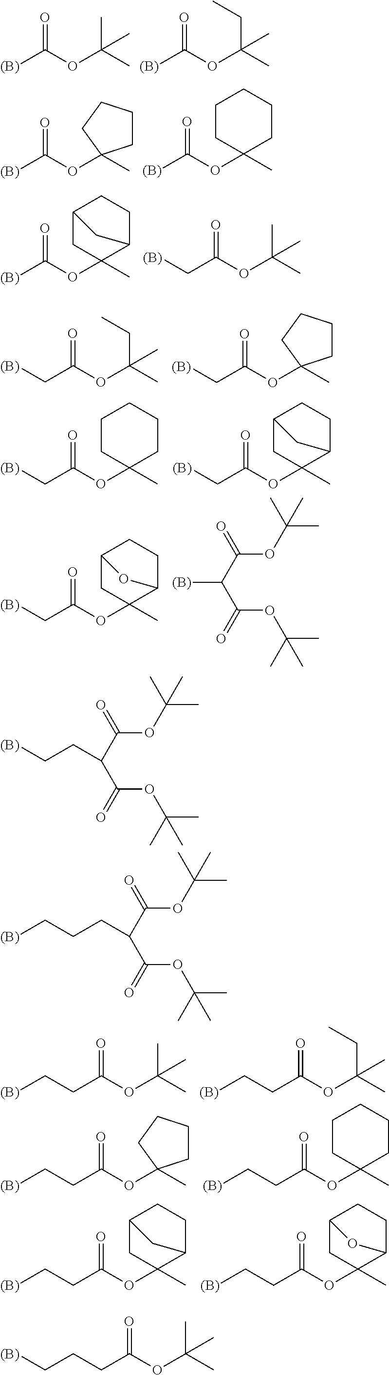
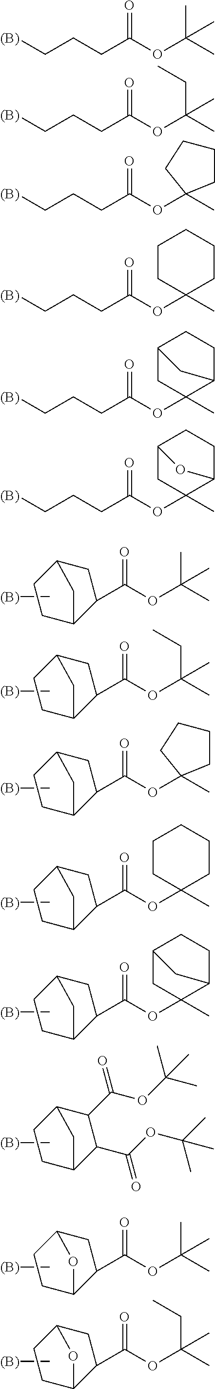
[0196]A monomer mixture comprising 9.9 g of phenyl trimethoxy silane (Monomer 100), 13.6 g of methyl trimethoxy silane (Monomer 101), 38.1 g of tetramethoxy silane (Monomer 102), and 25.6 g of the boric acid derivative shown by “Monomer 120” was heated under a nitrogen atmosphere at 100° C. for 3 hours to obtain a boron-containing silane mixture after confirmation of disappearance of the boric acid derivative by GPC. After cooling down to a room temperature, this mixture was gradually added into a mixture comprising 120 g of methanol, 1 g of methanesulfonic acid, and 60 g of deionized water over 30 minutes at room temperature; and then, after completion of the gradual addition, the resulting mixture was kept at 20° C. for 24 hours to carry out the hydrolysis condensation. After the reaction, 100 g of propylene glycol ethyl ether (PGEE) was added thereinto, and then, by-produced alcohols were distilled out under reduced pressure. Then, 1,000 mL of ethyl acetate was added thereinto to...
synthesis example a-4
[0198]A monomer mixture comprising 27.2 g of methyl trimethoxy silane (Monomer 101), 38.1 g of tetramethoxy silane (Monomer 102), and 11.1 g of the boric acid derivative shown by “Monomer 123” was gradually added into a mixture comprising 120 g of methanol, 1 g of methanesulfonic acid, and 60 g of deionized water over 30 minutes at room temperature; and then, after completion of the gradual addition, the resulting mixture was kept at 20° C. for 24 hours to carry out the hydrolysis condensation. After the reaction, 100 g of propylene glycol ethyl ether (PGEE) was added thereinto, and then, by-produced alcohols were distilled out under reduced pressure. Then, 1,000 mL of ethyl acetate was added thereinto to separate the water layer. To the remaining organic layer was added 100 mL of ion-exchanged water; and the resulting mixture solution was stirred, settled, and then separated into the layers. This operation was repeated for three times. The remaining organic layer was added with 200...
PUM
| Property | Measurement | Unit |
|---|---|---|
| Boiling point | aaaaa | aaaaa |
| Contact angle | aaaaa | aaaaa |
| Carrier mobility | aaaaa | aaaaa |
Abstract
Description
Claims
Application Information