Methods of end point detection for substrate fabrication processes

a technology of end point detection and substrate, which is applied in the direction of fluid pressure measurement, cleaning using liquids, instruments, etc., can solve the problems of compromising the integrity of features formed thereon, unable to stop the etching process by a predetermined time, and conventional end point detectors for plasma etching cannot operate reliably

Inactive Publication Date: 2013-08-01
APPLIED MATERIALS INC
View PDF2 Cites 213 Cited by
  • Summary
  • Abstract
  • Description
  • Claims
  • Application Information

AI Technical Summary

Benefits of technology

[0017]In still another embodiment, a method for determining the completion of a process and analyzing an end point of the process performed within a substrate processing chamber includes performing the process to remove a material from an interior portion of the substrate processing chamber, wherein the process generates a by-product and detecting the by-product in a space (e.g., a pressure cavity) near a support pedestal disposed in the interior portion of the substrate processing chamber concurrently while the process is being performed. In addition, a value of a property of the by-product is monitored and the end point of the process is determined when the value of the property of the by-product decreases below a threshold limit, which is determined when a maximum derivative value of the value of the property of the by-product is reached. In one aspect, the by-product generated in the space near the substrate and the support pedestal is directed to an analyzer coupled to the substrate processing chamber to determine and monitor the value of the property (e.g., optical densities, electrical fields, mass, fluorescence, and plasma emission, among others.) of the by-product. In another aspect, the by-product is water (e.g., ionized or gaseous water vapor)
[0018]In yet another embodiment, a method for analyzing an end point of an etching process performed inside an etch chamber includes detecting the generation of a by-product of the process in a space inside the etch chamber during the process performed to remove a material from a surface of a substrate disposed above a support pedestal, and monitoring a value of a property of the by-product. The method further includes determining the end point of the process by an analyzer coupled to the etch chamber when the value of the property of the by-product decreases below a threshold limit. In one aspect, the threshold limit is determined when a maximum derivative value of the value of the property of the by-product is reached.
[0019]In still...

Problems solved by technology

Otherwise, the material may flake off and deposit on a substrate, thereby compromising the integrity of features formed thereon.
Stopping the etching process by a predetermined time is not practical because of the differences in film thickness on the surface of a wafer substrate and small surface area of active devices on a small portion of the substrate.
However, conventional end point detectors for plasma etch do not operate reliably during deep trench processes and when device surface areas are small.
Also, as line widths become narrower, maintaining the laser focus upon a bottom of a trench is becoming difficult.
During the time when the chamber cleaning operation is performed, the production of semiconductor devices cannot continue.
However, it is difficult to correctly detect the end point of the cleaning ope...

Method used


Image

  • Methods of end point detection for substrate fabrication processes
  • Methods of end point detection for substrate fabrication processes
  • Methods of end point detection for substrate fabrication processes

Examples


example 1

EXAMPLE 1

Removal of a Native Oxide Material from the Surface of a Substrate or a Chamber Body

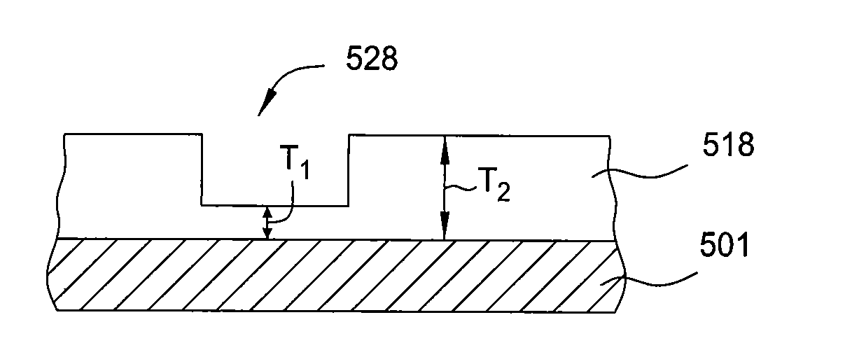
[0093]In one example, an oxide etching process may be performed to remove a silicon oxide material or a native oxide material (the oxide that forms from exposure to normal atmosphere on a silicon or other reactive material surface) from the surface of a substrate. Such a process can also be used to clean or condition the chamber and remove an oxide containing material from the chamber walls, chamber body, substrate support surface and other area inside the chamber.

[0094]The oxide etching process or oxide removal process described herein is also suitable for selective material removal. Examples of selective material removal (the removal of materials reactive to one etching / removal agent while other surrounding materials are not reacting and not being removed) includes, for example, removal of a material having different thicknesses in different surface area of the surface of a substrate, or ...

example 2

EXAMPLE 2

Removal of a Pad Oxide Material

[0107]During substrate fabrication, a pad oxide material layer formed on a small portion of the surface of a gate structure is generally required to be etched and removed before depositing the next material layer. On a typical patterned wafer substrate surface, the surface area of the pad oxide material layer is relatively small such that these pad oxide materials are difficult to etch and remove without formation of undesirable divot structures.

[0108]An oxide removal process is used to etch a pad oxide material from the surface of the substrate prior to depositing a gate oxide layer. The etching process may use etching gasses, such as a mixture of ammonia (NH3) and nitrogen trifluoride (NF3) gases. Factors which need to be considered in establishing the duration of the ideal etch process time include: the thickness of the gate oxide layer to be removed, the geometry of the substrate being cleaned, the volume capacity of the plasma, the volume...

example 3

EXAMPLE 3

Removal of a Copper Oxide Material During Chamber Conditioning

[0116]Before or after a copper deposition process inside a substrate processing chamber, it is desired to remove a copper oxide material from the substrate processing chamber so that the chamber can be ready for use with the copper oxide material initially absent from the chamber. A hydrogen gas (H2) is delivered into the chamber and a plasma is ignited to generate a hydrogen-containing plasma and clean and condition the chamber.

[0117]A chamber conditioning process or a metal material removal process is used to remove a copper oxide material from the surface of the chamber walls, substrate susceptor, and various portions of the chambers, before depositing a metal layer, such as a copper layer. In one embodiment, the metal material removal process may be a process used to remove a metal layer that contains a material including copper, tungsten, titanium, cobalt, nickel, tantalum, palladium, platinum or combinatio...


PUM

PropertyMeasurementUnit
Pressureaaaaaaaaaa
Thicknessaaaaaaaaaa
Pressureaaaaaaaaaa

Abstract

Methods and substrate processing systems for analyzing an end point of a process are provided. By-products of the process are detected and monitored to determine the completion of various types of reaction processes within a substrate processing chamber. The methods provide real time process monitoring, thereby reducing the need to rigidly constrain other substrate processing parameters, increasing chamber cleaning efficiency, and/or increasing substrate processing throughput.

Description

BACKGROUND OF THE INVENTION[0001]1. Field of the Invention[0002]The invention generally relates to methods for forming semiconductor devices and more particularly relates to methods for processing a semiconductor substrate surface.[0003]2. Description of the Related Art[0004]In the field of integrated circuit and flat panel display fabrication, multiple deposition and etching processes are performed in sequence on the substrate within one or more processing chambers to form various design structures. Processes such as etching, physical vapor deposition (PVD), chemical vapor deposition (CVD), chamber cleaning and conditioning, etc. are well known in the industry and each process requires appropriate ways to detect the completion of the desired reaction inside a substrate processing chamber and cleaning of residue build-up on the substrate or the wall of the substrate processing chamber.[0005]In general, silicon oxide, silicon nitride, metal oxide, or metal containing materials are de...

Claims


Application Information

Patent Timeline
IPC IPC(8): B44C1/22B08B7/00B08B7/04C23C16/52B05C5/00
CPCC23C14/54C23C14/564C23C16/52C23C16/4404C23C16/4401
Inventor ZHENG, BOCHANG, MEISUNDARRAJAN, ARVIND
Owner APPLIED MATERIALS INC
Why Eureka
Try Eureka